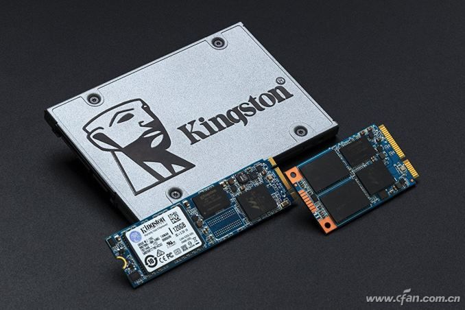
Recently, SSDs have continued to cut prices and many small partners have lit up the hope that they can finally upgrade their computers. However, the final capacity is a major obstacle, the current main capacity is still about 240GB, in fact, is nothing more than to do system disk. But now, larger-capacity solid particles are on the horizon, and the only trouble is the legendary slag life. However, do you really understand it?

The evolution of solid-state flash memory
The flash memory used in SSDs has undergone four changes: SLC, MLC, TLC, and the latest QLC. It must be said that the largest number of writes must be SLC, but the capacity of a single particle is too small and has been eliminated. MLC and TLC are also such step-by-step replacement relationships, and the capacity of each replacement generation is greatly increased. At the same time, the number of writes will decrease by one gear.
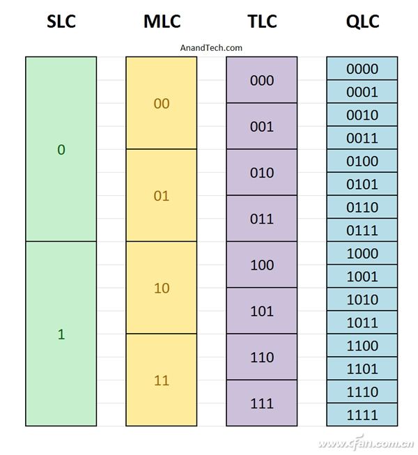
SLC: Fully-named Single-Level Cell, each Cell stores 1 bit of information, that is, only 0, 1 two voltage changes, the structure is simple, voltage control is also fast, reflecting the characteristics of long life, high performance, P / E life Between 10,000 and 100,000 times, the disadvantage is low capacity and high cost. After all, a Cell unit can only store 1 bit of information.
MLC: The full name is Multi-Level Cell. It is actually corresponding to SLC. NAND flash memory outside SLC is MLC type, and we often say MLC refers to 2bit MLC. MLC stores 2 bits of information per cell. The voltage has four variations of 000, 01, 10, and 11. Therefore, it requires more complex voltage control than SLC. The compression process takes longer, which means that the write performance is reduced. At the same time, reliability has also dropped. P/E life varies from 3000 to 5000 times depending on the process, and some are even lower.
TLC: TLC is Trinary-Level Cell, exactly 3 bit MLC, each cell unit stores 3 bits of information, there are 8 changes in voltage from 000 to 111, the capacity is increased by 1/3 again than MLC, the cost is lower, but the architecture is more Complex, long P/E programming time, slow write speed, and P/E life expectancy reduced to 1000-3000 times, and in some cases, lower.
QLC: The emergence of the Quad-Level Cell architecture has been further improved to 4 bit/cell, supporting 16 charging values, and the capacity can easily reach TB level. However, it is the slowest and the shortest. The initial life of P/E was only 300 times!
But do you think this means that QLC is the residue in the slag? This is not the case in reality.
Save 3D NAND for QLC Phoenix Nirvana
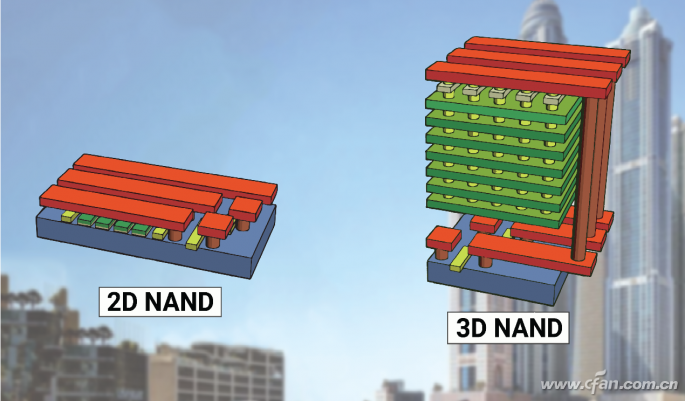
Today's NAND flash memory has entered the 3D NAND era. It is completely different from the 2D NAND era. The SLC, MLC, TLC, and even the early QLC we just talked about are based on the results of 2D NAND. The QLC for 3D NAND is the Phoenix Nirvana, and it's not just 300 times P/E slag flash.
In the era of 2D NAND flash memory, in order to pursue the improvement of the flash memory capacity, it is necessary to upgrade the process technology. This means that the process technology of the processor is continuously upgraded. More transistors are integrated with more advanced processes to increase the density, thereby increasing the capacity of the cell. cut costs.
What restricts the lifespan of Flash P/E is precisely because of continuous improvement of process technology. Smaller process technology leads to “more and more thinnessâ€, and reliability decreases. However, in the 3D NAND era, upgrading the flash memory capacity is not based on the micro process technology, but on the stack layer number (which can be understood as superposition), so the process becomes less important, even with the older process technology. Larger capacity flash memory.
Because of this, QLC flash memory has obtained different treatment from TLC. For example, now QLC flash memory from Micron and Intel directly uses 3D NAND technology, and the P/E lifetime reaches 1,000 times. Can you worry about it?
Another point is that as technology advances, such as error correction techniques, etc., the number of P/E writes to flash memory is not static. For example, TLC flash memory undergoes more advanced error correction techniques, and P/E is less than the initial 500 times. Now it has reached a level of 1000+, and so will QLC.
After QLC uses 3D NAND technology, the inherent short board is gone. On the contrary, its large-capacity advantage is further brought into play. The TB-class civilian SSDs in the future must rely on QLC support. Perhaps at this time next year, the TB solid-state price will be cheaper. coming.

ZGAR Aurora 1800 Puffs
ZGAR electronic cigarette uses high-tech R&D, food grade disposable pod device and high-quality raw material. All package designs are Original IP. Our designer team is from Hong Kong. We have very high requirements for product quality, flavors taste and packaging design. The E-liquid is imported, materials are food grade, and assembly plant is medical-grade dust-free workshops.
Our products include disposable e-cigarettes, rechargeable e-cigarettes, rechargreable disposable vape pen, and various of flavors of cigarette cartridges. From 600puffs to 5000puffs, ZGAR bar Disposable offer high-tech R&D, E-cigarette improves battery capacity, We offer various of flavors and support customization. And printing designs can be customized. We have our own professional team and competitive quotations for any OEM or ODM works.
We supply OEM rechargeable disposable vape pen,OEM disposable electronic cigarette,ODM disposable vape pen,ODM disposable electronic cigarette,OEM/ODM vape pen e-cigarette,OEM/ODM atomizer device.

Aurora 1800 Puffs,ZGAR Aurora 1800 Puffs Pod System Vape,ZGAR Aurora 1800 Puffs Pos Systems Touch Screen,ZGAR Aurora 1800 Puffs Disposable Vape Pod System,1800Puffs Pod Vape System
ZGAR INTERNATIONAL(HK)CO., LIMITED , https://www.oemvape-pen.com