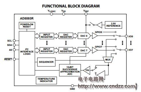
The AD5593R integrates eight I/O pins that can be individually configured as DAC outputs, ADC inputs, digital outputs, or digital inputs. When the I/O pin is configured as an analog output, it is driven by a 12-bit DAC. The DAC output range is 0 V to VREF, or 0 V to 2 x VREF. When the I/O pin is configured as an analog input, it is connected to a 12-bit ADC through an analog multiplexer. The ADC input range is 0 V to VREF, or 0 V to 2 × VREF. The I/O pins can also be configured as general purpose digital input or output (GPIO) pins. The GPIO pin status can be set or read back by accessing the GPIO registers via an I2C write/read operation.
The AD5593R integrates a 2.5V, 20 ppm/°C reference (default off) and a temperature indicator (indicating chip temperature). The temperature value is read back as part of the ADC read sequence.
The AD5593R is available in 2mm x 2mm WLCSP and 16-lead 3mm x 3mm LFCSP packages and operates over the -40°C to +105°C temperature range.
AD5593R features:
1, configurable 8-channel ADC / DAC / GPIO
2, can be configured as any combination of the following
3, 8 12-bit DAC channels
4, 8 12-bit ADC channels
5, 8 general purpose I/O pins
AD5593R application:
1. Control and monitoring
2, general purpose analog and digital I / O
Internal function diagram of AD5593R:

Figure 1: Internal Functional Diagram of the AD5593R
AD5593R Datasheet: Download now
More schematics and PCB code:
SHENZHEN CHONDEKUAI TECHNOLOGY CO.LTD , https://www.siheyidz.com