As sophisticated lithography technology continues to realize more transistors on a certain chip area, the level of digital technology is also constantly improving. These advances will have a huge impact on RF and microwave design. For example, high-speed analog-to-digital converters (ADCs) have paved the way for the implementation of software-defined radio (SDR) architectures. SDRs are widely used in many applications from cellular base stations to military radios. Thanks to the high-performance digital-to-analog converter (DAC), complex waveforms with high precision and wide dynamic range can be generated.
Looking at ADC and DAC from performance
From the performance point of view, ADC and DAC are one of the most diverse electronic component products. A converter can be selected from various performance indicators such as clock rate, frequency range, bit resolution, noise level, power consumption and dynamic range. Converter products include low-frequency 24-bit resolution converters for audio applications, lower resolution and lower frequency converters for control applications, and high-resolution, high-performance converters for medical, military, and wireless communication applications. For such products, a basic trade-off is accuracy and frequency: the wider the desired frequency range, the lower the available bit resolution. For example, the frequency of a 24-bit ADC and DAC is around 100 kHz, while the highest resolution of a converter operating at 1 GHz is about 16 bits.
Ideally, after the analog signal enters the ADC and is transmitted to a DAC with the same bandwidth and accuracy, the analog signal output from the DAC should be equal to the original signal. However, like analog devices, digital devices are subject to physical and manufacturing limitations, including: substrate and conductor signal loss, manufacturing tolerances, and signal attenuation due to impedance mismatch as part of the conversion process. In addition, the bit resolution of the converter determines the number of digital states used to describe the analog signal. For the DAC, the waveform reconstructed by 256 digital states is closer to the original signal waveform than the waveform reconstructed by 1 * bit) digital states. However, some applications may require only a few digital bits of resolution. Cost is another trade-off when choosing ADCs and DACs. The higher the bit resolution, the higher the cost.
The least significant bit (LSB) of the converter determines the minimum step size that can be divided into the peak or full-scale voltage range of the converter. It can also be used as a measure of converter bit accuracy, expressed by two parameters, differential nonlinearity (DNL) and integral nonlinearity (INL). There is only one LSB difference between two consecutive output codes of an ideal ADC, and the DNL value is zero. However, the gain and phase changes caused by the circuit and packaging of the converter will cause a certain degree of deviation of the least significant bit. Therefore, the LSB of the ADC and DAC will be affected to a certain extent in real applications. This is measured by the DNL and INL specifications. deviation. Maxim's application note 641 includes glossaries related to converters (including concise definitions of DNL and INL); in addition, Maxim's application manual 283 describes the measurement methods of DNL and INL.
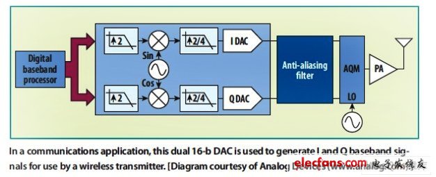
As portable electronic devices are increasingly used for personal and professional purposes, converter manufacturers are constantly looking for new design strategies to improve performance while reducing power consumption. Taking AD9125 of Analog Devices (ADI) as an example, this solution integrates two DACs in one package. The AD9125 is ideal for wireless infrastructure applications, such as generating in-phase (I) and quadrature (Q) digitally modulated baseband signal components in cellular base stations. This 16-bit converter has a sampling rate of 1GSPS and can support multi-carrier signals from cellular base stations. generate. The DAC has a flexible CMOS interface (see figure). The signal output from the dual DAC device can be filtered and then fed to an analog quadrature modulator (AQM), which is then amplified by a power amplifier and transmitted at the cellular site. This dual DAC device produces a 70MHz IF output at 800MSPS sampling frequency, which can achieve a spurious-free dynamic range (SFDR) of -72dBc. At the same sampling rate, for 100MHz output, two-tone intermodulation distortion (IMD) is -81dBc. In terms of accuracy, the typical values ​​of DNL and INL of AD9125 are ± 2.1LSB and ± 3.7LSB, respectively.

Figure: In communications applications, this dual-channel 16-bit DAC is used to generate in-phase (I) and quadrature (Q) baseband signals for use by wireless transmitters.
Copper-Clad Aluminum Core Wire,Copper Clad Aluminum Metal Wire,Copper Clad Aluminum Pure Copper Wire ,Copper Clad Aluminum Bimetallic Wire
changzhou yuzisenhan electronic co.,ltd , https://www.yzshelectronics.com