1 Introduction to RC56D / SP and TMS320F206
RC56D / SP is a 56k modem chip produced by Conexant (formerly Rockwell). RC56D / SP includes an 8-bit microcontroller (MCU) and a data pump (MDP), which is implemented by executing firmware solidified in 1Mbit (128K × 8) RAM and 2Mbit (ROM / Flash ROM. The device uses TCM Mesh coding technology, compatible with AT commands, supports V.42 modem link access protocol (LAPM) and MNP10 error correction protocol, and supports V.80 synchronous transmission protocol. In synchronous mode, the transmission clock can use internal, external and slave There are three clock modes, and the built-in phase-locked loop has a clock extraction function.It can extract the clock signal that is completely in the same frequency and phase as the clock sent by the peer from the received synchronous data stream as the receive clock of itself and DTE. K / s synchronization rate.
TMS320F206's CPU clock frequency is 20MHz, which has rich on-chip and off-chip resources, and has powerful asynchronous and synchronous serial ports.

Its asynchronous serial port has a full-duplex transmission and reception operation with the maximum transmission rate. Data transmission is completed through the transmission pin (TX) on the transmitter and the reception pin (RX) on the receiver. Through the asynchronous serial port control register (ASPCR), the four I / O ports IO0 ~ IO3 can be configured as handshake control signals to improve the signal transmission quality. [next]
The sending and receiving of its synchronous serial port both involve a 4-level first-in first-out (FIFO) buffer. By reducing the number of transmit or receive interrupts that occur during transmission, the FIFO buffer can reduce CPU unlocking (when sending or receiving data). The operation clock of the synchronous serial port can be generated internally or from an external clock source. When the internal clock mode is used, the maximum rate of sending and receiving operations is the CPU clock frequency divided by 2. When the external clock source is used, the data transmission rate will change with the external clock source.
The data sending and receiving operations of the synchronous serial port must be started by sending the corresponding frame synchronization pulse (FSX) and receiving frame synchronization pulse (FSR). FSX can be produced either internally or externally. FSR must be generated externally.
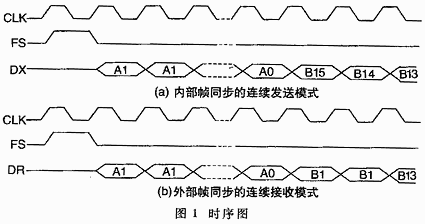
The synchronous serial port has continuous and burst operation modes, which can support a series of applications. In continuous mode, only one frame sync pulse is needed to continuously send or receive multiple software packages; in burst mode, only one 16-bit word is allowed to be sent or received after each frame sync pulse. The continuous transmission timing with internal frame synchronization and the continuous reception timing with external frame synchronization are shown in Figure 1 (a) and Figure 1 (b), respectively.
The synchronous serial port has two hardware interrupts: transmit interrupts (XINTs) and receive interrupts (RINTs), which informs the processor that the FIFO buffer needs service. By properly setting the interrupt generation conditions, the data can be sent and received continuously.
2 Hardware circuit design and working principle
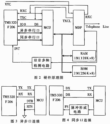
The block diagram of the system hardware circuit is shown in Figure 2. The modem uses the asynchronous connection synchronous transmission working mode, that is, the connection is performed in the asynchronous mode, and the synchronous transmission state is entered after the connection is established. Because TMS320F206 and MCU are TTL level, they can be directly connected. The specific connection of asynchronous serial port and synchronous serial port is shown in Figure 3 and Figure 4. Modem asynchronous and synchronous data use the same data port on the MCU. Therefore, the data on the sending pin of the MCU is the data that will be sent from the DTE, and the data on the receiving pin is the demodulated peer data, so the asynchronous or synchronous data transmission (TXD) and reception (RXD) of the TMS320F206 ) Pins are connected accordingly. Since the MCU asynchronous function is only used for modem setting and connection, the flow control function may not be used, that is, the handshake signal may not be used. Therefore, the RTS and DTR pins of the MCU are grounded to make them effective for a long time. [next]
TMS320F206 data transmission adopts external clock, internal frame synchronization and continuous mode. Reception adopts external clock and connection mode, and the received frame synchronization pulse is generated by MCU control. When the modem establishes a connection and the MCU receives the first frame of data, the control pulse forming circuit generates a single pulse with the same pulse width as the synchronous receive clock cycle, and starts the TMS320F206 to receive data. Because the system also sends a monitoring signal to protect the connection status when there is no useful data, unless the transmission is interrupted, the data reception will not stop once started. The transmit clock (TXCLK) and receive clock (RXCLK) of TMS320F206 are provided by the modem.

Modem sending clock is divided into three ways: internal, external and slave clock. They can be set by the AT & X0 (1,2) command. When set to internal clock, the modem sending clock is provided by the internal oscillation circuit of the modem chip. The internal oscillation circuit can produce any nominal frequency between 300 and 56 kHz. When the external clock mode is used, the external clock XTCLK is first sent to the MDP and MDP. On the one hand, it is used as the synchronous transmission clock of this chip. It is sent to the MCU and TMS320F206 as a synchronous transmission clock. Because the internal phase locked loop of the MDP can only be locked at any nominal frequency, the XTCLK frequency must be at any nominal frequency between 300 and 33.6 kHz. When using the slave clock mode, the modem will use the clock extracted from the received data stream as the transmit clock, that is, the local transmit clock is the same as the peer transmit clock. This modem uses an external clock for transmission.
The modem synchronous receive clock is provided by the local MDP. MDP can extract the clock signal RXCLK that is exactly the same as the send clock of the peer from the received data stream, and use it as the receive clock of itself and MCD and TMS320F206. [next]
3 Modem working mode setting
The default working mode of the modem is different squinting mode. If you want to make it into synchronous working mode, you must set it through AT command. The AT commands that we use to set the synchronization mode are as follows: + ES, + ESA, & Q1, and & X1. The + ES command is used to enable or disable the synchronous transmission mode. The + ESA command is used to set some related characteristics of the synchronous transmission mode, such as whether to use cyclic redundancy code check, whether to use reverse non-return to zero code transmission, etc. The & Q1 command is used to control the modem to be an asynchronous connection synchronous transmission mode, that is, the modem is connected in an asynchronous manner, and once connected, it immediately enters the synchronous transmission mode. The & X1 command is used to select the external clock as the modem sending clock.
The connection process of the modem varies with the application of the system. When transmitting through the public switched telephone network, the modem can be connected by automatic answering. At this time, the modem is divided into a calling end and a called end. The calling terminal initiates the call, that is, dials the called party user number. The called-end modem starts the answering process by detecting the ringing current. The called-end automatic answering method can be started by the ATS0 = N (N = 1 ... 255) command, where N represents how many ringing current signals are detected to start the answering process, N = 0 disable auto answer function.
When the system does not transmit through the public telephone exchange network, because there is no ringing signal on the line, the pseudo-automatic answering method is adopted. The so-called pseudo-automatic answering means that the DSP program controls the modem to answer, rather than the modem itself starting the answering process. The principle of implementation is as follows: a dual tone multi-frequency (DTMF) tone detection circuit is designed at the line port of the called end. When the calling end initiates a call, it only needs to dial any dual tone multi-frequency number, and the tone detection circuit detects the signal After the tone, a square wave pulse signal is generated, and the INT1 interrupt of TMS320F206 is decoded. After the TMS320F206 enters the interrupt service program, it sends an ATA (Forced Answer) command to the modem to start the answer process and establish a connection with the opposite modulator. Because there is no dial tone on the line, and the default state after the modem is reset requires the dial tone provided by the switching equipment to dial, so when initializing the calling-end modem, the ATX1 command must be added. This command allows the modem to dial directly without dial tone. Modem dialing operation can be executed by ATD *** (*** represents the dialed number) command.

4 System workflow
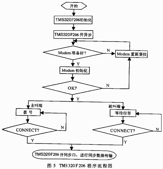
TMS320F206 program flowchart is shown in Figure 5. The system workflow is as follows: After the system is powered on and reset, TMS320F206 first initializes, opens the asynchronous port, and then checks whether the modem is ready. If it is not ready, reset the modem again; if it is ready, send AT command to enter the modem to initialize the modem. Namely, the modem synchronization port can be named, and the modem can be set to the asynchronous connection synchronous transmission mode, using an external clock and setting related characteristics such as synchronous transmission mechanism and transmission rate. At the same time, it is determined whether the calling terminal adds the ATX1 command and what answering method the called terminal adopts. Every time the modem receives the correct AT command and performs the corresponding operation correctly, it returns an OK signal through the asynchronous serial port. Therefore, if the TMS320F206 receives an OK signal, it indicates that the initialization was successful. After the initialization of the modem is completed, the calling terminal dials to start the call, and the called terminal enters the automatic answering or pseudo-automatic answering process. After connecting, the modem will send CONNECT message back to TMS320F206. After that, TMS320F206 prohibits the asynchronous port, opens the synchronous port, and starts synchronous data transmission.
After the development of this synchronous modem was completed, synchronous transmission tests were carried out on dedicated lines, public telephone lines and power-carrying lines, and all achieved relatively good transmission effects. When the analog channel is needed to complete the synchronous transmission and transmission, especially at the access layer, this modem will have a wide range of uses.
KW3-Basic Micro Switch-Lever Type
KW3-Basic Micro Switch-Lever Type
Ningbo Jialin Electronics Co.,Ltd , https://www.donghai-switch.com