Abstract: The base station system (BTS) needs to meet various standards while meeting the signal link specifications. This article introduces some signal link devices, such as: high dynamic performance ADC, variable gain amplifier, mixer and local oscillator, details their use in a typical base station, can meet the base station's high dynamic performance, high cut Point performance and low noise requirements.
Most word receivers have higher requirements for the high-performance analog-to-digital converter (ADC) and analog devices they use. For example, cellular base station digital receivers require sufficient dynamic range to handle larger interfering signals, thereby demodulating useful signals at lower levels. Maxim's 15-bit 65Msps analog-to-digital converter MAX1418 or 12-bit 65Msps analog-to-digital converter MAX1211 with a 2GHz MAX9993 or 900MHz MAX9982 integrated mixer can provide excellent dynamic characteristics for the receiver's two-stage critical circuit , Maxim's intermediate frequency (IF) digital adjustable gain amplifier (DVGA) MAX2027 and MAX2055 can provide a higher third-order output intercept point (OIP3) in many systems and meet the required gain adjustment range of the system.
A cellular base station (BTS: base transceiver station) is composed of multiple different hardware modules, one of which is a transceiver (TRx) module that performs RF reception (Rx) and transmission (Tx) functions. In the old analog AMPS and TACS BTS, one transceiver can only be used to handle one full-duplex Rx and Tx RF carrier. To achieve the required call coverage, many transceivers are needed to provide enough carriers. Today, analog technology has been replaced by CDMA and WCDMA globally, and Europe has adopted GSM 10 years ago. In CDMA, multiple callers use the same RF frequency, so that a transceiver can simultaneously process the signals of multiple callers. Up to now, there are a variety of CDMA and GSM design solutions, and BTS manufacturers have also been committed to exploring ways to reduce costs and power consumption. Optimizing a single carrier solution or developing a multi-carrier receiver is an effective solution. Figure 1 is a structural block diagram of an undersampling receiver commonly used in BTS equipment.
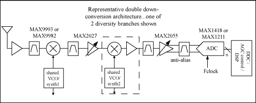
Figure 1. Block diagram of an undersampling receiver
In Figure 1, Maxim's 2GHz MAX9993 and 900MHz MAX9982 mixers provide the gain and linearity required for many designs and have extremely low coupling noise, which eliminates the need for passive mixers with higher losses . The MAX2027 and MAX2055 operate at the first and second IF stages of the receiver. Both devices can achieve + 40dBm OIP3 over their entire gain adjustment range. In the circuit in Figure 1, the data converter uses MAX1418 (15-bit, 65Msps) and MAX1211 (12-bit, 65Msps). In addition, Maxim's data converter products have other sampling rate devices that can meet most design requirements. If the second down converter in FIG. 1 is omitted (shown in dashed lines), then the circuit shown in FIG. 1 becomes a single-channel down converter structure. Maxim's low-noise ADC: The undersampling receiver structure shown in Figure 1 of the MAX1418 has strict requirements on the noise and distortion of the ADC. In the receiver, the low-level useful signal is digitized alone or accompanied by a useless large-scale signal that needs extra attention. Therefore, to make the receiver work properly, the effective noise figure of the ADC should be based on these two signals. The extreme case (that is, the minimum useful signal and the maximum unnecessary signal) are calculated. For small analog input signals, thermal noise and quantization noise dominate the noise floor of the ADC, which determines the ADC's noise figure (NF).
In fact, once the effective noise figure of the ADC under small signal conditions is determined, the cascaded noise figure of the analog circuit (RF or IF) is also determined accordingly. The minimum power gain of the ADC pre-stage circuit should meet the noise figure requirements of the receiving circuit. Generally, the power gain value is limited to the maximum blocking level or the highest interference level that the receiver can tolerate before the ADC is overloaded. In BTS, if automatic gain control (AGC) is not used, the dynamic range of ADC generally cannot meet the requirements of both circuit noise figure (receiver sensitivity) and maximum blocking. , AGC circuit can also be included in the two-stage circuit.
Other products in the MAX1418 series are particularly suitable for baseband applications with fINPUT = fCLOCK / 2. When the converter works in this frequency range, using these devices with excellent baseband characteristics will have the best dynamic range. These products include the MAX1419 for 65Msps clock rate and the MAX1427 for 80Msps clock rate, and their baseband SFDR (spurious free dynamic range) can reach 94.5dBc.
Table 1 lists the main technical parameters of MAX1418:
Table 1. MAX1418 electrical characteristics
When LSB is not connected, the MAX1418 can also work with a 14-bit interface device. In this way, there will be a slight loss in SNR while SFDR is not affected.
Figure 2 shows the noise distribution of the ADC without blocking. It is assumed that the total cascaded noise figure of all analog circuits before the ADC is 3.5dB, and the design goal is that the degradation of the total noise figure caused by the ADC does not exceed 0.2dB. To meet the sensitivity requirements of CDMA base station receivers. Such a noise figure value should leave sufficient margin for the air interface, but the final result depends on the Eb / No (bit energy to noise power spectral density ratio) requirement of the final detector. Based on the thermal noise + quantization noise floor of MAX1418 in Table 1, when the device clock is 61.44Msps (50x chip rate), its equivalent noise figure is 26.9dB. Due to the process gain control, the ADC noise in the 1.23MHz CDMA channel bandwidth is 14dB lower than the ADC noise in the Nyquist broadband. In general, in order to obtain a receiver cascade noise figure of 3.7dB, the total gain should reach 36dB.
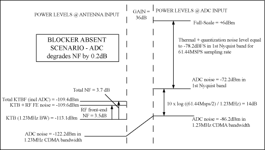
Figure 2. ADC noise distribution without blocking
When the ADC front-end gain is 36dB, the single-tone blocking level of more than -30dBm at the antenna end will exceed the input range of the ADC. The cdma2000® cellular base station standard stipulates that the maximum blocking level allowed at the antenna end is -30dBm. At this time, the front-end gain needs to be reduced by 6dB, so that the maximum blocking signal added to the ADC is allowed within the margin allowed by the standard specification. Bigger. Assuming a 2dB margin, a 6dB reduction in front-end gain can make the maximum blocking level at the antenna end become -26dBm, and the maximum allowable input signal of the ADC becomes + 4dBm (see Figure 3). When single-tone blocking occurs, the cellular standard allows the total interference (noise + distortion) to deteriorate by 3dB relative to the reference sensitivity, but it is left to the designer how this 3dB is allocated between noise and distortion.
Assumption: When a blocking signal occurs, the AGC gain is 6dB. The design allows RF front-end cascading noise plus distortion to reduce NF by 1dB (nominal value is 3.5dB). When the front-end gain of the ADC is only 30dB, the SNR of the ADC determines its effective noise figure of 29.4dB, and the noise figure of the cascaded receiver under 'blocking conditions' is 5.7dB, which is higher than the 3.7dB calculated based on the receiver sensitivity The noise figure is 2dB lower. Since the spurious characteristics are not taken into account in this calculation, the ADC's spurious-free dynamic range (SFDR) also allows an additional 1dB reduction. When there is a blocking signal, SINAD can be used to calculate the effective NF instead of calculating the noise and SFDR base values ​​separately.
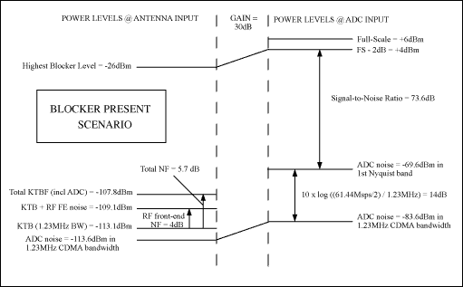
Figure 3. ADC noise response in the presence of blocking MAX1211 allows a down-conversion structure. If sufficient SNR and SFDR specifications can be obtained in the higher IF section, an undersampling circuit can be used for the down-conversion structure. Maxim's MAX1211 12-bit, 65Msps converter is designed using this structure. Its pins are compatible with the upcoming 80Msps and 95Msps converters. This series of devices can directly sample the input signal IF number up to 400MHz. In addition, , It also has other advanced performance, such as the clock input can be a differential signal or a single-ended signal, the clock duty cycle can be between 20% and 80%, in addition, there is also a data valid indicator (to simplify the clock and Data timing), using a small 40-pin QFN (6mm x 6mm x 0.8mm) package, two's complement and Gray code digital output format. Table 2 lists the typical AC characteristics of the MAX1211 when the analog input frequency is 175MHz.
Table 2. MAX1211 electrical characteristics
Compared with the double frequency conversion structure, the primary converter has obvious advantages. Since the second-stage down-conversion mixer, the second-stage IF gain circuit and the second-stage LO synthesizer are omitted, the number of components and board space can be reduced by about 10%, and the cost can be saved by $ 10 to $ 20. The stray considerations of different structures If you need to further save the number of components, circuit board space, reduce power consumption and cost, you can use the primary frequency conversion structure given below. Assume that the designed cdma2000 receiver works in the PCS band, the sampling rate is 61.44Msps, the synthesizer reference frequency is 30.72MHz, the center of the first intermediate frequency is selected at the 6th order Nyquist band 169MHz, and the bandwidth is about 1.24MHz. For the DDS structure, the same first intermediate frequency of 169MHz is used, and the center frequency of the second intermediate frequency is in the second-order Nyquist band of 46.08MHz.
Table 3. Hypothetical spurious characteristics for SDC and DDC architectures
Table 3 lists the RF carrier spur search assumptions near the upper end of the PCS band when using a single carrier, one down conversion (SDC), and two down conversion (DDC) structures. For the SDC structure, the spur search can find 134 harmonic components in the RF receiving frequency band, receiving image frequency band, IF frequency band and IF image frequency band. Most of these spurious signals are of higher order and will not reduce the receiving performance. For the DDC structure, the spurious search will find more than 2400 harmonic components, which is more than 18 times that found under the SDC structure. These harmonics are distributed in the RF receiving frequency band, receiving image frequency band, and first-level IF frequency band. , The first-level IF image frequency band, the second-level IF frequency band and the second-level IF image frequency band. Spurious signals originating from higher-order clock harmonics and the reference frequency of the synthesizer can be suppressed by carefully considering the layout of the circuit board or adding filtering in the design, but the suppression of a large number of lower-order spurious components Is more difficult. Maxim's IF amplifiers: MAX2027 & MAX2055Maxim also provides numerically controlled gain, high-performance IF amplifiers with 1dB increments per stage. The MAX2027 is a digitally controlled gain amplifier (DVGA). It uses single-ended input / single-ended output and can work in the frequency range of 50MHz to 400MHz. Its noise figure at maximum gain is only 5dB. The MAX2055 is a single-ended input / differential output DVGA that can drive high-performance ADCs in the 30MHz to 300MHz frequency range. A booster transformer can be used between the differential output of the MAX2055 and the differential input of the ADC. The transformer provides differential drive, which is beneficial to the balance between the output signals. These two DVGAs work at 5V bias and have an OIP3 of + 40dBm over the entire gain setting range. For more details, please refer to the relevant information on the Maxim website (). Maxim's high-linear mixer: MAX9993 & MAX9982 In the receiving circuit, the mixer often withstands a larger input signal with stricter performance requirements. Under ideal conditions, the amplitude and phase of the mixer output signal are proportional to the amplitude and phase of the input signal, and this proportional relationship is independent of the LO signal. According to this assumption, the amplitude response of the mixer has a linear relationship with the RF input and is independent of the LO input signal.
However, the non-linearity of the mixer will produce some undesired mixing signals, called spurious responses. These spurious signals are the response of the IF band generated by the undesired signals that reach the RF port of the mixer. . Useless spurious signals will interfere with the operation of useful RF signals. The IF frequency of the mixer can be given by:
fIF = ± mfRF ± nfLO Here, IF, RF and LO are the signal frequencies of the respective ports, m and n are the harmonic order after mixing the RF and LO signals.
Integrated (or active) balanced mixers (such as Maxim ’s MAX9993 and MAX9982) have received much attention because of their performance over passive mixing schemes. When m or n is an even number, the balanced mixer can suppress a certain spurious response, and the second harmonic performance is more excellent. An ideal double-balanced mixer can suppress all responses where m or n (or both) are even. In a double-balanced mixer, the IF, RF, and LO ports are all isolated from each other. Using a properly designed unbalanced transformer, the mixer can overlap in the IF, RF, and LO bands. Features of MAX9993 and MAX9982 include: low noise figure, built-in LO buffer, low LO drive, LO switch that allows two LO inputs, excellent LO noise characteristics, etc. In addition, RF unbalance is integrated on the RF and LO ports transformer.
Maxim's mixers have embedded LO buffers with excellent LO noise performance, reducing the LO power requirements. Usually LO noise mixed with higher level input blocking signal will reduce the receiving sensitivity. The MAX9993 and MAX9982 contain low-noise LO buffers to reduce the impact on reception sensitivity when blocking occurs. For example, assuming that the sideband noise of the VCO input signal is -145dBc / Hz, the typical value of the MAX9993's LO noise characteristic is -164dBc / Hz, so that the composite sideband noise only drops by 0.05dBc / Hz to -144.95dBc / Hz. Using this method, the user not only provides a low-level LO signal to the mixer, but also ensures that the mixing characteristics of the receiver are not degraded by the performance of the MAX9993's built-in LO buffer.
In addition, there is a tricky second-order spurious response, also known as half-IF (1/2 IF) spurious response. For low-end injection, the mixer order is: m = 2, n = -2; High-end injection, mixer order: m = -2, n = 2. At low-end injection, the input frequency that causes the half-IF spurious response is fIF / 2 lower than the desired RF frequency (Figure 4). The desired RF frequency is 1909MHz mixed with the LO frequency of 1740MHz, and the resulting IF frequency is 169MHz. Although the RF and IF carrier bandwidth of CDMA is 1.24MHz, it is expressed here as a single-frequency signal with the center carrier frequency. In this example, the unwanted signal with a frequency of 1824.5MHz causes a half-IF spurious component of 169MHz:
verification:
2 x fHalf-IF-2 x fLO =
2 x (fRF-fIF / 2)-2 x (fRF-fIF) =
2 x (fRF-2 x fIF / 2)-2 x fRF + 2 x fIF = fIF
From this we can get:
2 x 1824.5MHz-2 x 1740MHz = 169MHz
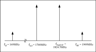
Figure 4. Location of useful fRF, fLO, fIF and useless fHalf-IF frequencies
The total amount of suppression (also called 2x2 spurious response) can be predicted from the second intercept point IP2 of the mixer. Figure 5 shows the 2x2 IMR or spur value (MAX9993 data from Maxim). Note: The signal level in the figure is the mixer input level calculated with the input IP2 (IIP2) performance.
The specific calculation formula is as follows: IIP2 = 2 x IMR + PSPUR = IMR + PRF
= 2 x 70dBc + (-75dBm) = 70dBc + (-5dBm)
= + 65dBm Because the typical spurious response 2RF-2LO provided by Maxim ’s MAX9982 900MHz active filter is 65dBc, the IIP2 calculation method is as follows: IIP2 = 2 x IMR + PSPUR = IMR + PRF
= 2 x 65dBc + (-70dBm) = 65dBc + (-5dBm)
= + 60dBm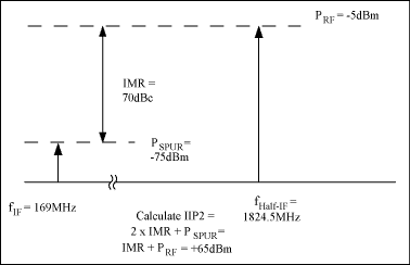
Figure 5. Calculate the second intercept point of the mixer input signal, IIP2
The image frequency suppression of the RF channel is close to the front end of the mixer and is used to attenuate all amplifier harmonics, while the noise filter of the LO path is used to attenuate the harmonics caused by LO injection. Higher-level input signals will cause distortion or intermodulation at the input or output of the device, and the value can be obtained by calculating the intercept point. When the LO power of the mixer is a fixed value, the order of its intercept point or distortion component depends only on the RF frequency doubling, and has nothing to do with the frequency doubling of the LO, and only needs to consider the change of the RF signal. The order mentioned here represents the rate at which distortion increases as the input level rises.
When the receiver gain requirement is not high, Maxim's 15-bit ADC MAX1418 has excellent noise performance, so it can withstand a large blocking level or interference level with the smallest AGC. The MAX1211 ADC series products are suitable for the primary conversion receiving structure, and its first IF input frequency can reach 400MHz. In addition, Maxim's MAX9993 and MAX9982 mixers can provide the required linearity, while the noise figure is low and the power gain is high, so passive filters can be omitted in the receiver design process. The MAX2027 and MAX2055 DVGA have a typical OIP3 value of approximately + 40dBm over the entire adjustable gain range. A receiver consisting of these components can improve the performance of a low-cost solution by one level.
1. The output cutoff point of the circuit or system under test is the sum of the input cutoff point and the gain (in dB).
References The following application notes can be downloaded from the Maxim website: AN 728 'Defining and Testing Dynamic Parameters in High-Speed ​​ADCs, Part 1' AN 729 'Dynamic Testing of High-Speed ​​ADCs, Part 2' AN 1197 'How Quantization and Thermal Noise Determine an ADC's Effective Noise Figure 'AN1929' Understanding ADC Noise for Small and Large Signal Inputs for Receiver Applications 'AN 1838' Mixer 2x2 spurious response and IP2 'AN 2021' Specifications and Measurement of Local Oscillator Noise in Integrated Circuit Base Station Mixers 'AN 2371' Comparison of the performance of integrated RF mixer and passive mixer solutions '' Digital Techniques for Wideband Receivers 'by James Tsui, Artech House Publishers, 1995.' RF Design Guide, Systems, Circuits , and Equations' by Peter Vizmuller, Artech House Publishers, 1995 'CDMA Systems Engineering Handbook' by Jhong Sam Lee & Leonard E. Miller, Artech House Publishers, 1998.
Most word receivers have higher requirements for the high-performance analog-to-digital converter (ADC) and analog devices they use. For example, cellular base station digital receivers require sufficient dynamic range to handle larger interfering signals, thereby demodulating useful signals at lower levels. Maxim's 15-bit 65Msps analog-to-digital converter MAX1418 or 12-bit 65Msps analog-to-digital converter MAX1211 with a 2GHz MAX9993 or 900MHz MAX9982 integrated mixer can provide excellent dynamic characteristics for the receiver's two-stage critical circuit , Maxim's intermediate frequency (IF) digital adjustable gain amplifier (DVGA) MAX2027 and MAX2055 can provide a higher third-order output intercept point (OIP3) in many systems and meet the required gain adjustment range of the system.
A cellular base station (BTS: base transceiver station) is composed of multiple different hardware modules, one of which is a transceiver (TRx) module that performs RF reception (Rx) and transmission (Tx) functions. In the old analog AMPS and TACS BTS, one transceiver can only be used to handle one full-duplex Rx and Tx RF carrier. To achieve the required call coverage, many transceivers are needed to provide enough carriers. Today, analog technology has been replaced by CDMA and WCDMA globally, and Europe has adopted GSM 10 years ago. In CDMA, multiple callers use the same RF frequency, so that a transceiver can simultaneously process the signals of multiple callers. Up to now, there are a variety of CDMA and GSM design solutions, and BTS manufacturers have also been committed to exploring ways to reduce costs and power consumption. Optimizing a single carrier solution or developing a multi-carrier receiver is an effective solution. Figure 1 is a structural block diagram of an undersampling receiver commonly used in BTS equipment.

Figure 1. Block diagram of an undersampling receiver
In Figure 1, Maxim's 2GHz MAX9993 and 900MHz MAX9982 mixers provide the gain and linearity required for many designs and have extremely low coupling noise, which eliminates the need for passive mixers with higher losses . The MAX2027 and MAX2055 operate at the first and second IF stages of the receiver. Both devices can achieve + 40dBm OIP3 over their entire gain adjustment range. In the circuit in Figure 1, the data converter uses MAX1418 (15-bit, 65Msps) and MAX1211 (12-bit, 65Msps). In addition, Maxim's data converter products have other sampling rate devices that can meet most design requirements. If the second down converter in FIG. 1 is omitted (shown in dashed lines), then the circuit shown in FIG. 1 becomes a single-channel down converter structure. Maxim's low-noise ADC: The undersampling receiver structure shown in Figure 1 of the MAX1418 has strict requirements on the noise and distortion of the ADC. In the receiver, the low-level useful signal is digitized alone or accompanied by a useless large-scale signal that needs extra attention. Therefore, to make the receiver work properly, the effective noise figure of the ADC should be based on these two signals. The extreme case (that is, the minimum useful signal and the maximum unnecessary signal) are calculated. For small analog input signals, thermal noise and quantization noise dominate the noise floor of the ADC, which determines the ADC's noise figure (NF).
In fact, once the effective noise figure of the ADC under small signal conditions is determined, the cascaded noise figure of the analog circuit (RF or IF) is also determined accordingly. The minimum power gain of the ADC pre-stage circuit should meet the noise figure requirements of the receiving circuit. Generally, the power gain value is limited to the maximum blocking level or the highest interference level that the receiver can tolerate before the ADC is overloaded. In BTS, if automatic gain control (AGC) is not used, the dynamic range of ADC generally cannot meet the requirements of both circuit noise figure (receiver sensitivity) and maximum blocking. , AGC circuit can also be included in the two-stage circuit.
Other products in the MAX1418 series are particularly suitable for baseband applications with fINPUT = fCLOCK / 2. When the converter works in this frequency range, using these devices with excellent baseband characteristics will have the best dynamic range. These products include the MAX1419 for 65Msps clock rate and the MAX1427 for 80Msps clock rate, and their baseband SFDR (spurious free dynamic range) can reach 94.5dBc.
Table 1 lists the main technical parameters of MAX1418:
Table 1. MAX1418 electrical characteristics
| Parameter | CondiTIon | Symbol | Typ Value | Units |
| ResoluTIon | N | 15 | Bits | |
| Analog Input Range | VID | 2.56 | VP-P | |
| DifferenTIal Input Resistance | RIN | 1 | kΩ | |
| AC SpecificaTIons | fCLK = 65Msps | |||
| Thermal + Quantization Noise Floor | Analog input = -35dBFS | Nfloor | -78.2 | dBFS |
| Signal-to-Noise Ratio Analog in = -2dBFS | fIN = 70MHz | SNR | 73.6 | dB |
| Spurious-Free Dynamic Range Analog in = -2dBFS | fIN = 70MHz | SFDR | 84 | dB |
| Signal-to-Noise-and-Distortion Analog in = -2dBFS | fIN = 70MHz | SINAD | 73.3 | dB |
When LSB is not connected, the MAX1418 can also work with a 14-bit interface device. In this way, there will be a slight loss in SNR while SFDR is not affected.
Figure 2 shows the noise distribution of the ADC without blocking. It is assumed that the total cascaded noise figure of all analog circuits before the ADC is 3.5dB, and the design goal is that the degradation of the total noise figure caused by the ADC does not exceed 0.2dB. To meet the sensitivity requirements of CDMA base station receivers. Such a noise figure value should leave sufficient margin for the air interface, but the final result depends on the Eb / No (bit energy to noise power spectral density ratio) requirement of the final detector. Based on the thermal noise + quantization noise floor of MAX1418 in Table 1, when the device clock is 61.44Msps (50x chip rate), its equivalent noise figure is 26.9dB. Due to the process gain control, the ADC noise in the 1.23MHz CDMA channel bandwidth is 14dB lower than the ADC noise in the Nyquist broadband. In general, in order to obtain a receiver cascade noise figure of 3.7dB, the total gain should reach 36dB.

Figure 2. ADC noise distribution without blocking
When the ADC front-end gain is 36dB, the single-tone blocking level of more than -30dBm at the antenna end will exceed the input range of the ADC. The cdma2000® cellular base station standard stipulates that the maximum blocking level allowed at the antenna end is -30dBm. At this time, the front-end gain needs to be reduced by 6dB, so that the maximum blocking signal added to the ADC is allowed within the margin allowed by the standard specification. Bigger. Assuming a 2dB margin, a 6dB reduction in front-end gain can make the maximum blocking level at the antenna end become -26dBm, and the maximum allowable input signal of the ADC becomes + 4dBm (see Figure 3). When single-tone blocking occurs, the cellular standard allows the total interference (noise + distortion) to deteriorate by 3dB relative to the reference sensitivity, but it is left to the designer how this 3dB is allocated between noise and distortion.
Assumption: When a blocking signal occurs, the AGC gain is 6dB. The design allows RF front-end cascading noise plus distortion to reduce NF by 1dB (nominal value is 3.5dB). When the front-end gain of the ADC is only 30dB, the SNR of the ADC determines its effective noise figure of 29.4dB, and the noise figure of the cascaded receiver under 'blocking conditions' is 5.7dB, which is higher than the 3.7dB calculated based on the receiver sensitivity The noise figure is 2dB lower. Since the spurious characteristics are not taken into account in this calculation, the ADC's spurious-free dynamic range (SFDR) also allows an additional 1dB reduction. When there is a blocking signal, SINAD can be used to calculate the effective NF instead of calculating the noise and SFDR base values ​​separately.

Figure 3. ADC noise response in the presence of blocking MAX1211 allows a down-conversion structure. If sufficient SNR and SFDR specifications can be obtained in the higher IF section, an undersampling circuit can be used for the down-conversion structure. Maxim's MAX1211 12-bit, 65Msps converter is designed using this structure. Its pins are compatible with the upcoming 80Msps and 95Msps converters. This series of devices can directly sample the input signal IF number up to 400MHz. In addition, , It also has other advanced performance, such as the clock input can be a differential signal or a single-ended signal, the clock duty cycle can be between 20% and 80%, in addition, there is also a data valid indicator (to simplify the clock and Data timing), using a small 40-pin QFN (6mm x 6mm x 0.8mm) package, two's complement and Gray code digital output format. Table 2 lists the typical AC characteristics of the MAX1211 when the analog input frequency is 175MHz.
Table 2. MAX1211 electrical characteristics
| Parameter | Condition | Symbol | Typ Value | Units |
| Resolution | N | 12 | Bits | |
| Analog Input Range | VID | 2 | VP-P | |
| Differential Input Resistance | RIN | 15 | kΩ | |
| AC Specifications | fCLK = 65Msps | |||
| Thermal + Quantization Noise Floor | Analog input = -35dBFS | Nfloor | 69.3 | dBFS |
| Signal-to-Noise Ratio Analog in = -0.2dBFS | fIN = 32.5MHz fIN = 175MHz | SNR | 68.3 66.8 | dB |
| Spurious-Free Dynamic Range Analog in = -0.2dBFS | fIN = 32.5MHz fIN = 175MHz | SFDR | 82.4 79.7 | dB |
| Signal-to-Noise-and-Distortion Analog in = -2dBFS | fIN = 32.5MHz fIN = 175MHz | SINAD | 68.1 66.5 | dB |
Compared with the double frequency conversion structure, the primary converter has obvious advantages. Since the second-stage down-conversion mixer, the second-stage IF gain circuit and the second-stage LO synthesizer are omitted, the number of components and board space can be reduced by about 10%, and the cost can be saved by $ 10 to $ 20. The stray considerations of different structures If you need to further save the number of components, circuit board space, reduce power consumption and cost, you can use the primary frequency conversion structure given below. Assume that the designed cdma2000 receiver works in the PCS band, the sampling rate is 61.44Msps, the synthesizer reference frequency is 30.72MHz, the center of the first intermediate frequency is selected at the 6th order Nyquist band 169MHz, and the bandwidth is about 1.24MHz. For the DDS structure, the same first intermediate frequency of 169MHz is used, and the center frequency of the second intermediate frequency is in the second-order Nyquist band of 46.08MHz.
Table 3. Hypothetical spurious characteristics for SDC and DDC architectures
| SDC | DDC | Parameter | Value |
| x | x | Receive band | 1904.3800 to 1905.6200MHz |
| x | x | Clock Frequency | 61.44000MHz |
| x | x | Max clock harmonic | 30 |
| x | x | Synthesizer ref freq | 30.7200MHz |
| x | x | Max synthesizer harmonic | 40 |
| x | x | First injection LS | 1736.0000MHz |
| x | x | Max 1st LO harmonic | 5 |
| x | x | Receive image band | 1566.3800 to 1567.6200MHz |
| x | x | First IF band | 168.3800 to 169.6200MHz |
| x | Second injection LS | 122.9200MHz | |
| x | Max 2nd LO harmonic | 5 | |
| x | 1st IF image band | 76.2200 to 77.4600MHz | |
| x | Second IF band | 45.4600 to 46.7000MHz |
Table 3 lists the RF carrier spur search assumptions near the upper end of the PCS band when using a single carrier, one down conversion (SDC), and two down conversion (DDC) structures. For the SDC structure, the spur search can find 134 harmonic components in the RF receiving frequency band, receiving image frequency band, IF frequency band and IF image frequency band. Most of these spurious signals are of higher order and will not reduce the receiving performance. For the DDC structure, the spurious search will find more than 2400 harmonic components, which is more than 18 times that found under the SDC structure. These harmonics are distributed in the RF receiving frequency band, receiving image frequency band, and first-level IF frequency band. , The first-level IF image frequency band, the second-level IF frequency band and the second-level IF image frequency band. Spurious signals originating from higher-order clock harmonics and the reference frequency of the synthesizer can be suppressed by carefully considering the layout of the circuit board or adding filtering in the design, but the suppression of a large number of lower-order spurious components Is more difficult. Maxim's IF amplifiers: MAX2027 & MAX2055Maxim also provides numerically controlled gain, high-performance IF amplifiers with 1dB increments per stage. The MAX2027 is a digitally controlled gain amplifier (DVGA). It uses single-ended input / single-ended output and can work in the frequency range of 50MHz to 400MHz. Its noise figure at maximum gain is only 5dB. The MAX2055 is a single-ended input / differential output DVGA that can drive high-performance ADCs in the 30MHz to 300MHz frequency range. A booster transformer can be used between the differential output of the MAX2055 and the differential input of the ADC. The transformer provides differential drive, which is beneficial to the balance between the output signals. These two DVGAs work at 5V bias and have an OIP3 of + 40dBm over the entire gain setting range. For more details, please refer to the relevant information on the Maxim website (). Maxim's high-linear mixer: MAX9993 & MAX9982 In the receiving circuit, the mixer often withstands a larger input signal with stricter performance requirements. Under ideal conditions, the amplitude and phase of the mixer output signal are proportional to the amplitude and phase of the input signal, and this proportional relationship is independent of the LO signal. According to this assumption, the amplitude response of the mixer has a linear relationship with the RF input and is independent of the LO input signal.
However, the non-linearity of the mixer will produce some undesired mixing signals, called spurious responses. These spurious signals are the response of the IF band generated by the undesired signals that reach the RF port of the mixer. . Useless spurious signals will interfere with the operation of useful RF signals. The IF frequency of the mixer can be given by:
fIF = ± mfRF ± nfLO Here, IF, RF and LO are the signal frequencies of the respective ports, m and n are the harmonic order after mixing the RF and LO signals.
Integrated (or active) balanced mixers (such as Maxim ’s MAX9993 and MAX9982) have received much attention because of their performance over passive mixing schemes. When m or n is an even number, the balanced mixer can suppress a certain spurious response, and the second harmonic performance is more excellent. An ideal double-balanced mixer can suppress all responses where m or n (or both) are even. In a double-balanced mixer, the IF, RF, and LO ports are all isolated from each other. Using a properly designed unbalanced transformer, the mixer can overlap in the IF, RF, and LO bands. Features of MAX9993 and MAX9982 include: low noise figure, built-in LO buffer, low LO drive, LO switch that allows two LO inputs, excellent LO noise characteristics, etc. In addition, RF unbalance is integrated on the RF and LO ports transformer.
Maxim's mixers have embedded LO buffers with excellent LO noise performance, reducing the LO power requirements. Usually LO noise mixed with higher level input blocking signal will reduce the receiving sensitivity. The MAX9993 and MAX9982 contain low-noise LO buffers to reduce the impact on reception sensitivity when blocking occurs. For example, assuming that the sideband noise of the VCO input signal is -145dBc / Hz, the typical value of the MAX9993's LO noise characteristic is -164dBc / Hz, so that the composite sideband noise only drops by 0.05dBc / Hz to -144.95dBc / Hz. Using this method, the user not only provides a low-level LO signal to the mixer, but also ensures that the mixing characteristics of the receiver are not degraded by the performance of the MAX9993's built-in LO buffer.
In addition, there is a tricky second-order spurious response, also known as half-IF (1/2 IF) spurious response. For low-end injection, the mixer order is: m = 2, n = -2; High-end injection, mixer order: m = -2, n = 2. At low-end injection, the input frequency that causes the half-IF spurious response is fIF / 2 lower than the desired RF frequency (Figure 4). The desired RF frequency is 1909MHz mixed with the LO frequency of 1740MHz, and the resulting IF frequency is 169MHz. Although the RF and IF carrier bandwidth of CDMA is 1.24MHz, it is expressed here as a single-frequency signal with the center carrier frequency. In this example, the unwanted signal with a frequency of 1824.5MHz causes a half-IF spurious component of 169MHz:
verification:
2 x fHalf-IF-2 x fLO =
2 x (fRF-fIF / 2)-2 x (fRF-fIF) =
2 x (fRF-2 x fIF / 2)-2 x fRF + 2 x fIF = fIF
From this we can get:
2 x 1824.5MHz-2 x 1740MHz = 169MHz

Figure 4. Location of useful fRF, fLO, fIF and useless fHalf-IF frequencies
The total amount of suppression (also called 2x2 spurious response) can be predicted from the second intercept point IP2 of the mixer. Figure 5 shows the 2x2 IMR or spur value (MAX9993 data from Maxim). Note: The signal level in the figure is the mixer input level calculated with the input IP2 (IIP2) performance.
The specific calculation formula is as follows: IIP2 = 2 x IMR + PSPUR = IMR + PRF
= 2 x 70dBc + (-75dBm) = 70dBc + (-5dBm)
= + 65dBm Because the typical spurious response 2RF-2LO provided by Maxim ’s MAX9982 900MHz active filter is 65dBc, the IIP2 calculation method is as follows: IIP2 = 2 x IMR + PSPUR = IMR + PRF
= 2 x 65dBc + (-70dBm) = 65dBc + (-5dBm)
= + 60dBm

Figure 5. Calculate the second intercept point of the mixer input signal, IIP2
The image frequency suppression of the RF channel is close to the front end of the mixer and is used to attenuate all amplifier harmonics, while the noise filter of the LO path is used to attenuate the harmonics caused by LO injection. Higher-level input signals will cause distortion or intermodulation at the input or output of the device, and the value can be obtained by calculating the intercept point. When the LO power of the mixer is a fixed value, the order of its intercept point or distortion component depends only on the RF frequency doubling, and has nothing to do with the frequency doubling of the LO, and only needs to consider the change of the RF signal. The order mentioned here represents the rate at which distortion increases as the input level rises.
When the receiver gain requirement is not high, Maxim's 15-bit ADC MAX1418 has excellent noise performance, so it can withstand a large blocking level or interference level with the smallest AGC. The MAX1211 ADC series products are suitable for the primary conversion receiving structure, and its first IF input frequency can reach 400MHz. In addition, Maxim's MAX9993 and MAX9982 mixers can provide the required linearity, while the noise figure is low and the power gain is high, so passive filters can be omitted in the receiver design process. The MAX2027 and MAX2055 DVGA have a typical OIP3 value of approximately + 40dBm over the entire adjustable gain range. A receiver consisting of these components can improve the performance of a low-cost solution by one level.
1. The output cutoff point of the circuit or system under test is the sum of the input cutoff point and the gain (in dB).
References The following application notes can be downloaded from the Maxim website: AN 728 'Defining and Testing Dynamic Parameters in High-Speed ​​ADCs, Part 1' AN 729 'Dynamic Testing of High-Speed ​​ADCs, Part 2' AN 1197 'How Quantization and Thermal Noise Determine an ADC's Effective Noise Figure 'AN1929' Understanding ADC Noise for Small and Large Signal Inputs for Receiver Applications 'AN 1838' Mixer 2x2 spurious response and IP2 'AN 2021' Specifications and Measurement of Local Oscillator Noise in Integrated Circuit Base Station Mixers 'AN 2371' Comparison of the performance of integrated RF mixer and passive mixer solutions '' Digital Techniques for Wideband Receivers 'by James Tsui, Artech House Publishers, 1995.' RF Design Guide, Systems, Circuits , and Equations' by Peter Vizmuller, Artech House Publishers, 1995 'CDMA Systems Engineering Handbook' by Jhong Sam Lee & Leonard E. Miller, Artech House Publishers, 1998.
2.5 Small SATA SSD for PC Laptop
2.5'' SATAIII 6Gb/s SSD from Microbits
Incredible Performance:Sequential read and write up to 550MB/s and 500MB/s, 5 times faster than the traditional hard drive,accelerated by 3D NAND technology.
Compatible Devices: Compatible with desktops and laptops that accept 2.5" 7 millimeter SATA drives.
Trustworthy and Reliable:Supports TRIM command, Garbage Collection technology, RAID, and ECC (Error Checking & Correction) to provide the optimized performance and enhanced reliability.
SATA 3 2.5 inch SSD,Portable Usb C External Hard Disk,Laptop Hard Drive Enclosure,Hard Disk For Desktop Laptop,120Gb Hard Disk Memory
MICROBITS TECHNOLOGY LIMITED , http://www.microbitstrade.com