The core of this paper is: In the design of the C language platform that can reduce the structure exploration time, how to break through the new thinking in the structure? How to form a unique C language platform, is the SoC design optimized?
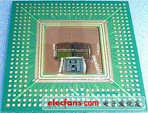
In the past, most semiconductor manufacturers used FPGA (Field Programmable Gate Array) to make samples (Prototype), and then locked several important specifications of the wafer to find the most suitable structure for the wafer. The biggest disadvantage of this method is that the operation time is very long. However, the design method of the C language platform is to use the software simulation analysis to review the structure of the wafer. In the past, the sample of the FPGA platform takes about half a year to explore the structure. If the design method of the C language platform is adopted, it only takes about 2 weeks. 1 month time.
The fastest development at present is Japan's OKI, the ARM-based integration platform and design environment can be applied to the advanced technology of wafer specialization. According to the planning of OKI, the SoC for C language platform design technology is used internally. The three architectures are: "μPLAT" + software, "μPLAT" + dedicated accelerator + software, hard wired circuit.
In the "μPLAT" + software part, traditional FPGAs also support this function, so IC design companies can use the IP core source's Process Core to develop SoC based on μPLAT. For example, ARM has already packaged ProcESS Core into software. Customer use. The part of the chip developed for "μPLAT" + dedicated accelerator + software and hard wired circuit structure is to use C language platform design to make development more efficient. In addition, in "μPLAT" + special accelerator (software) + software, the dedicated accelerator degree is also divided into two execution modes, namely: converting C language data into System C, and then inputting SySTem C into the action synthesis tool, and finally Embed a hard wired circuit and specialize the Process Core with compositing, and then perform C language calculations on the Process Core. By adopting the first mode of the synthetic action mode, the wafer can achieve a low power consumption effect, and the second specific process Core synthesis method is indeed quite effective from the viewpoint of resource sharing, but the power consumption is often inferior to the first. Kind of synthetic action.

Caption: Most semiconductor manufacturers use FPGAs to make samples, and find the most suitable structure for the wafer. The biggest disadvantage of this method is that the operation time is very long. (School of Computer Science)
C language platform to get rid of traditional stereotypes
The flow of the SoC design method for the C language platform is that it is first necessary to receive the request from the client, the "C language/C++ description calculation" processed by the SoC, and the "use case" of the SoC usage method, and receive the "calculus" (Algorithm) ) Test environment" Then start the SoC development work. In this case, it is necessary to check the source code (Source Code) to confirm whether it is suitable for action synthesis or combination of software. If it is not suitable, review the revision of the source code to discuss the structure. Since the project has been given the role of "high-precision evaluation", it has already got rid of the stereotype of the traditional "design". At this time, the priority of short-term mass production is higher than the quality, for example, the design that completes the exploration within one month, only The verification of the representative project can shorten the verification time of the exploration project, and the verification quality is maintained by the design method after the exploration.
The structural exploration project is further divided into: a review of the draft structure and the production and testing of the initial model of the structure. The review of the draft structure is based on the analysis of the source code, and it is decided to use the "mechanical connection of action synthesis" or a dedicated processor. For chips with less complex functions, when low production cost and low power consumption are required, most of the motion synthesis methods are selected; when similar functions are required for composite processing, a dedicated processor mode is usually selected. Immediately after the basic policy is decided, the width of the numerator, the structure of the parallel processing circuit, the operating frequency, the collocation with the software, and so on, and then the structural model of the wafer is fabricated, and then verified by a virtual prototyping simulator. In addition to the wafer function, the simulator can analyze all the performance of the whole system and the chip including data transfer outside the wafer.
Using the C language platform design method, it takes only 2 weeks to 1 month to complete the simulation analysis and review the structure of the wafer. (NaTIonal Center for Ecological Analysis and Synthesis)
We are a factory who professional for Mono Solar Cells,Solar Cells Materials Used,Monocrystalline Solar Cell,Mono Crystalline Solar Cell. Most of our modules are customized as the clients requests. We have 400W to 550W half cells solar panel. Sure. custom is ok. Welcome to your inquiry and tell me your requests. Let's talk the details.

Mono Solar Cells,Solar Cells Materials Used,Monocrystalline Solar Cell,Mono Crystalline Solar Cell
Jiangxi Huayang New Energy Co.,Ltd , https://www.huayangenergy.com