Like all digital circuits, glitch is a thorny problem in FPGA circuits. Its appearance can affect the stability and reliability of circuit operation, and it can lead to malfunction and logic disorder of the entire digital system.
There must be a delay when the signal is wired through the logic unit in the FPGA device. The size of the delay is not only related to the length of the connection and the number of logic cells, but also related to the manufacturing process, operating voltage, temperature, etc. of the device. In addition, the high-low level conversion of the signal also requires a certain transition time. Due to the two factors, when the level value of the multi-channel signal changes, at the moment of signal change, the output of the combinatorial logic has a sequence, not At the same time, there are often some incorrect spikes, which are “burrsâ€. Any combination of circuits, feedback circuits and counters is possible.
Potential glitch signal generator.
The length of the circuit wiring is different, which causes the input signal delay of each port to be inconsistent. There is competition and risk, and glitch will occur. Distributed capacitors and inductors between discrete components can filter out these spurs, so when designing circuits with discrete components, competitive risk and glitch problems are rarely considered, but there are no distributed capacitors and inductors inside the PLD/FPGA, and no glitch can be filtered out (even if Less than 1 ns).
Give a simple example:

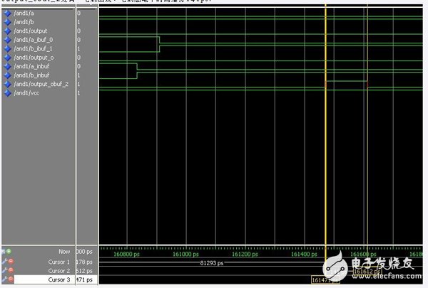
Design a two-input AND gate, output<=A & B; perform post-layout simulation (no support pin constraint file at this time) to see:

There is a glitch at output_obuf_2. The glitch is high for 141ps.


From the output_obuf to the output output, although the glitch is eliminated, it cannot be guaranteed to be eliminated in other cases. I think there may be a reason that the glitch time is relatively small here, so the output at the output is normal.
The first occurrence of the glitch is due to the change of input A from 1 to 0 and B from 0 to 1.

As can be seen from the static timing file: A, B arrives at the gate with a time difference of 141ps, which is the reason for the glitch in the above.
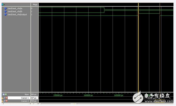
Add the pin constraint file to the following simulation:

It can be seen that there is a significant glitch in the output output.
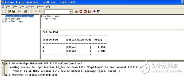
Timing analysis report:

For signal A: (Trace delay of A) + AND gate internal delay = 9.139ns;
For signal B: (Trace delay of B) + AND gate internal delay = 5.607ns;
That is, A and B arrive at the door with a difference of 3.532 ns. The figure below shows that the glitch time coincides exactly.

Glitch is not harmful to all inputs, such as the D input of the trigger, as long as the data does not appear on the rising edge of the clock, and meets the data establishment and retention time, it will not cause harm to the system, and when the glitch A logic error occurs when the signal becomes the system's enable signal, control signal, handshake signal, trigger clear signal, preset signal, clock signal, or latch input signal. Therefore, judging whether there is an adventure in the logic circuit and how to avoid the risk is a problem that the designer must consider.
Wall Box And Outlet,Wall Box Outlet,Electrical Box Outlet,Electrical Box Vs Outlet
Huizhou Fibercan Industrial Co.Ltd , https://www.fibercannetworks.com