Li Jian, deputy of the National People's Congress and secretary of the Party Committee of Wuhan University, served as the leader of the national semiconductor lighting engineering leading group. He believed that it is necessary to write a low-carbon economy into the government work report, and suggested that with the advent of the low-carbon economy era, it is necessary to further accelerate development. Semiconductor lighting industry.
Li Jian said that semiconductor lighting is a revolution in the field of lighting following incandescent and fluorescent lamps. Compared with traditional incandescent lamps and fluorescent lamps, semiconductor lighting has obvious power saving effects, so it is of great significance for developing a low-carbon economy, especially for promoting low-carbon life. Last year, China's lighting electricity consumption was 430 billion kWh, accounting for 12% of the country's total electricity consumption. If a quarter of users use semiconductor lighting, they can save hundreds of billions of dollars a year and reduce tens of millions of tons of carbon dioxide emissions.
After the country started the semiconductor lighting project in 2003, the industry developed rapidly, and the total output value is expected to reach 100 billion yuan this year. In order to promote this high-tech industry closely related to people's livelihood to develop better and faster, and grow into a strategic emerging industry, Li Jian suggested that the first is to introduce policies to encourage the use of semiconductor lighting energy-saving lamps as soon as possible, to purchase semiconductor lighting energy-saving lamps. The financial sector gives appropriate appropriate subsidies to accelerate the entry of semiconductor lighting into thousands of households. Second, we must increase the intensity of key technologies in the semiconductor lighting industry, and strive to master the core technologies with independent intellectual property rights. The third is to promote development by application and accelerate the demonstration of “Ten Cities and Ten Thousand Cities†organized and implemented by the Ministry of Science and Technology. Fourth, we must pay more attention to standards and testing to ensure product quality and promote the healthy development of this emerging industry.

PCB Prototype
PCB Prototype Specification:
In the process of developing a Printed Circuit Board-based solution for your company? This can be an extremely time-consuming, labor-intensive process where there is a high degree of uncertainty in the outcome. Developing a PCB prototype offers a fast, cost-effective option for getting your design from concept to production, while minimizing some of the risks associated with a Standard PCB service.
Prototype Printed Circuit Boards That Meet Our High Quality Standards:
BentePCB offers rapid PCB prototyping services in very good quality yet at a low cost. We're fully compliant with ISO9001:2008 quality management systems, and we have an in-house quality control department to verify that all work meets our high standards. Depending on your custom requirements, we can prototype your PCB within 3-7 days, compared to -18 days of Standard PCB service.
Check out our Circuit Board prototype capabilities in the following table:
|
Features |
Capability |
|
Quality Grade |
Standard IPC 2 |
|
Number of Layers |
1 - 16layers |
|
Order Quantity |
5pcs - 100pcs |
|
Build Time |
2 - 7 days |
|
Material |
FR-4 Standard Tg 140°C |
|
Board Size |
Min 6*6mm | Max 500*500mm |
|
Board size tolerance |
±0.1mm - ±0.3mm |
|
Board Thickness |
0.4mm - 2.0mm |
|
Board Thickness Tolerance |
±0.1mm - ±10% of thickness of board |
|
Copper Weight |
1.0oz - 2.0oz |
|
Inner Layer Copper Weight |
0.5oz - 1.0oz |
|
Copper Thickness Tolerance |
+0μm +20μm |
|
Min Tracing/Spacing |
5mil/5mil |
|
Solder Mask Sides |
As per the file |
|
Solder Mask Color |
Green, White, Blue, Black, Red, Yellow |
|
Silkscreen Sides |
As per the file |
|
Silkscreen Color |
White, Black |
|
Surface Finish |
Lead Free HASL - RoHS |
|
Min Annular Ring |
5mil |
|
Min Drilling Hole Diameter |
8mil |
|
Min Width of Cutout (NPTH) |
0.8mm |
|
NPTH Hole Size Tolerance |
±.002" (±0.05mm) |
|
Min Width of Slot Hole (PTH) |
0.6mm |
|
PTH Hole Size Tolerance |
±.003" (±0.08mm) - ±.006" (±0.15mm) |
|
Surface/Hole Plating Thickness |
20μm - 30μm |
|
SM Tolerance (LPI) |
.003" (0.075mm) |
|
Aspect Ratio |
1.10 (hole size: board thickness) |
|
Test |
10V - 250V, flying probe or testing fixture |
What Are the Benefits of Circuit Board Prototyping?
We recommend you chose PCB prototyping service for function testing of new products prior to making a commitment to a full-production run. Benefits of developing PCB board prototype include:
• Rapidly test and correct designs if there is any mistake
• Opportunity to detect potential design flaws in the early stages
• Quick turnaround time helps you achieve your productivity goals
• Low-quantity production runs featuring a minimum order quantity of only one boards
• Lower production tolerances provide a clear indication of how well the finished PCB will perform
Once your prototype boards demonstrated their ability to meet your quality and performance requirements, it is ready for a full production run. Then we will transition to Standard PCB service. It provides tighter production tolerances and more advanced options including free Design for Manufacture (DFM) check that is capable of detecting potential issues which could reduce the quality of your PCB.
About Us:
BentePCB is a professional PCB manufacturing which is focus on double side, multilayer, HDI PCB , rigid PCB and Flexible PCB mass production. The company was established on 2011.
We have two factories together, The factory in Shenzhen is specialized in small and middle volume orders and the factory in Jiangxi is for big volumn.
Why Us?
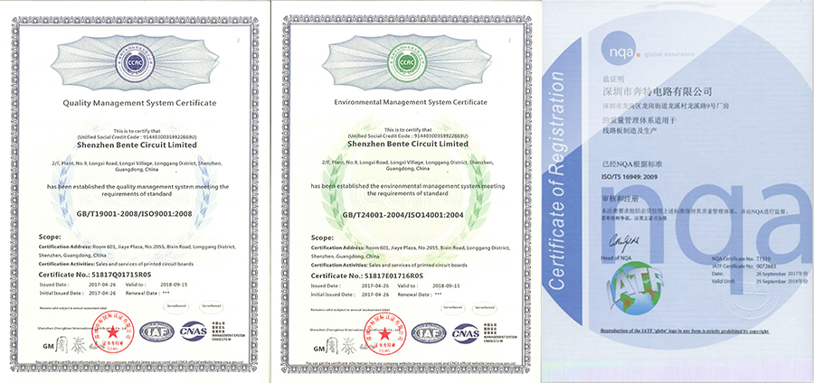
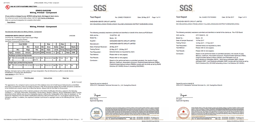
UL (E492586), ISO9001, ISO14001, TS16949, RoHS certified.
Turnover USD 10-50 million per year.
15,000 sqm area, 450 staff .
Mass Production from single to 16 layers.
Special Material:ROGERS, Arlon, Taconic.etc.
Client:Huawei, SAMSUNG, Malata, Midea,Texas Instruments.etc.
Certification(UL:E492586, TS16949, ISO14001, ISO9001,RoHS):
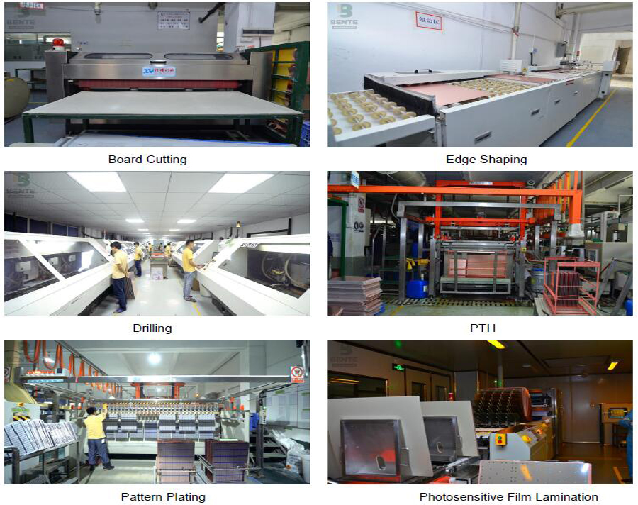
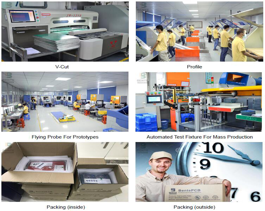
Factory Tour:
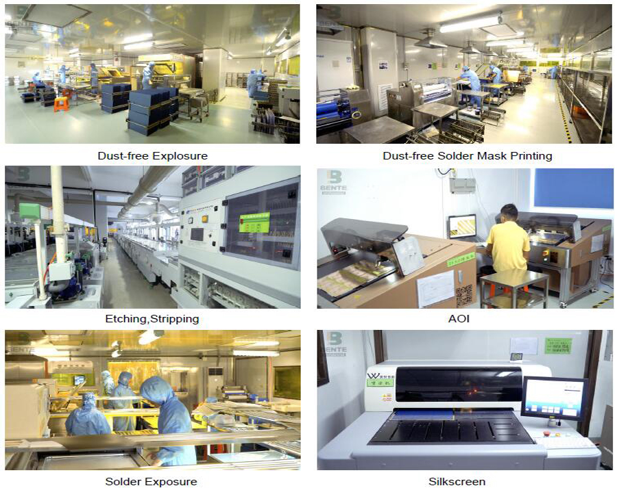
Exhibition:
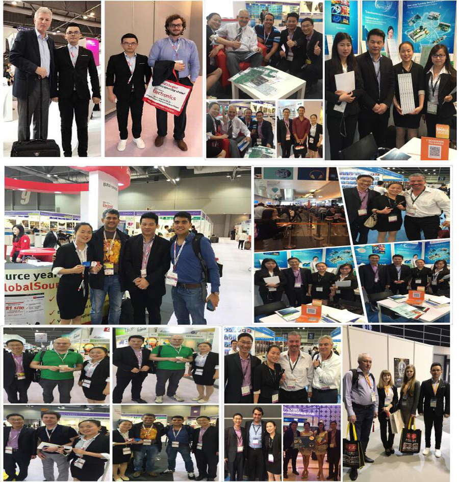
We Took part in the famous exhibitions over the past years,and got highly appreciation from the top experts,as well as cooperated tightly with them.
Delivery:
BentePCB offers flexible shipping methods for our customers, you may choose from one of the methods below.

FAQ:
Q1: What does BentePCB need for a customized PCB order?
A: The customers need to provide Gerber or pcb file.If you do not have the file in the correct format, you can send all the details related to the products.
Q2: What is your quotation policy?
A: For the PCB order in large quantity, BentePCB will send you the quotation based on the MOQ of the products concerned, and the price will be reasonable with good quality.
Q3: How long will you send us quotation ?
A: After all files were sent, 2 to 8 hours as per your file.
Q4:What is your minimum order quantity?
A:Our MOQ is 1 PCS.
Q5: How about the service BentePCB offered to the customers?
A: If you have any questions about our products or company, do not hesitate to send us your inquiry toour customer service representatives, Your satisfaction is our pursuits.

We don`t just sell PCBs .We sell sleep.

PCB Prototype
PCB Prototype,Prototype PCB Assembly,PCB Assembly Prototype,PCB Circuit Board Prototype
Shenzhen Bente Circuit Limited , http://www.bentegroup.com