In order to realize the access to SDRAM memory in embedded system design, this paper proposes a design scheme of SDRAM controller based on AMBA-AHB bus specification. The scheme first introduces the AMBA bus specification briefly, and then gives the implementation principle of SDRAM controller and detailed sub-module division based on the overall framework design of the entire storage controller. The entire controller design has been implemented in Verilog HDL language and passed Modelsim simulation and FPGA verification. The simulation results show that the designed controller complies with the internal instruction operation of SDRAM and meets strict timing requirements.
0 PrefaceWith the development of large-scale integrated circuits and high-speed, low-power, high-density storage technologies, SDRAM dynamic memories have become the mainstream of PC memory due to their large capacity, high speed, and low price. However, the internal control logic of the SDRAM memory is very complicated, and the timing requirements are also very strict. Therefore, it is necessary to design a special SDRAM controller to realize the system access to the SDRAM.
The memory controller is the interface between the AMBA-AHB bus and the off-chip storage device in the embedded microprocessor, and completes the data transmission of the bus master device (CPU or DMA) and off-chip storage device (SDRAM or SRAM), its function and performance. It determines the type of external memory supported by the embedded microprocessor and the access speed of the external memory, which in turn determines the processing speed of the entire embedded system. The AMBA bus specification has become the standard for embedded on-chip bus in microprocessors. The design is based on the AMBA bus standard. The storage controller IP supporting the common memory types of embedded systems has great practical significance.
1 Introduction to AMBA BusA typical AMBA bus-based microcontroller architecture is shown in Figure 1.
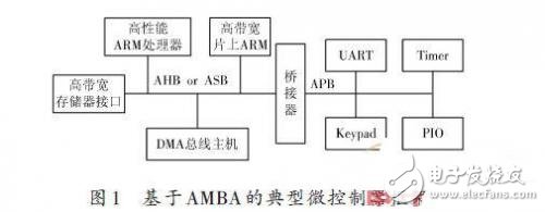
It contains an AHB (Advanced High-Performance Bus) or ASB bus as a system skeleton that enables large amounts of data communication between the CPU or DMA module and off-chip memory to achieve large bandwidth.
In addition, there is a bridge on this high-performance bus to connect low-bandwidth APBs, while most of the system peripherals are connected to the APB. Users can independently design microprocessors and peripheral IPs based on this specification, improving system development efficiency and module reusability.
Among them, the AHB bus is a high-performance bus supporting multi-bus masters for high-performance, high-clock-frequency systems, which ensures an effective connection between the processor and off-chip memory. A complete AHB transmission process can be divided into an address transmission phase and a data transmission phase. The address transmission phase transmits addresses and control signals, while the data transmission phase transmits read and write data and response signals. The AHB bus supports pipeline transmission, which means that the next address transmission phase can be performed simultaneously in the previous data transmission phase, and different transmission phases can be overlapped to improve the data processing speed of the system.
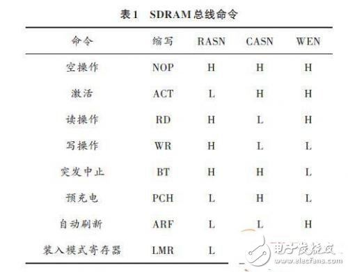
2 SDRAM working principleSDRAM is a high-speed and high-capacity synchronous dynamic memory. Compared with static memory such as SRAM, it has the advantages of large capacity, high speed and low price. It is a commonly used data memory in image processing. However, due to the particularity of the SDRAM memory structure, it is necessary to continuously perform precharge, refresh, and the like on the SDRAM to keep data from being lost. The internal operation of the SDRAM is implemented by bus commands, which are jointly generated by the RASN, CASN, and WEN signals, as shown in Table 1 (H indicates a high level and L indicates a low level).
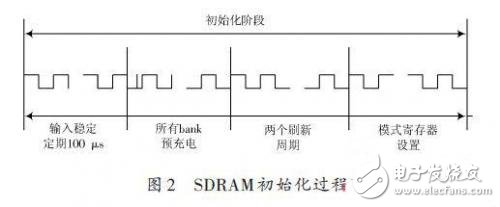
After the SDRAM is powered up, it must be initialized in a certain way. The memory does not accept any commands other than NOP for 100 μs after power-up stabilization. After 100μs, the precharge command is issued to all banks of the SDRAM through the controller, so that all banks of the SDRAM enter the standby state. After that, two automatic refresh operations are continuously performed on the SDRAM, so that the internal refresh of the SDRAM chip and the counter enter a normal running state. After the two refresh cycles are completed, the SDRAM mode register (Mode Register) is operated. The mode register is used to determine which operating mode the SDRAM will operate. The entire initialization process is shown in Figure 2.
The design is based on the slave module of the AMBA-AHB bus. The SDRAM controller is located between the on-chip AHB bus and the off-chip memory device, and is suspended as a slave on the AHB bus. It needs to communicate with the AHB bus through the AHB bus interface module, so it must comply with the AHB bus standard; the other side needs to provide control signals to the external storage device to achieve read and write operations to the external storage device. The controller receives a data transfer request from the bus master that conforms to the AMBA-AHB bus specification, and generates a correct read and write control signal to the SDRAM memory to complete the data transfer request of the bus.
The AMBA 2.0 bus defines a set of on-chip bus standards for embedded microcontrollers, so this design is an independently designed peripheral IP based on this specification.
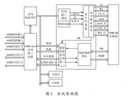
4 SDRAM controller system design architectureThe connection relationship between the SDRAM controller and the AHB bus interface in the whole system is shown in FIG. 3.
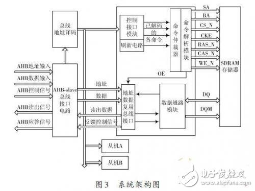
The AHB-slave bus interface circuit is used to implement signal transmission between the SDRAM control logic and the AHB-master.
According to the AMBA bus specification, when the AHB bus slave (slave) is on the rising edge of the bus clock and the HREADY signal (issued by the slave) is high, the bus control signal, data signal, address signal, etc. from the AHB bus must be latched. For internal decoding modules and other modules.
4.2 Bus Address Decoding
The AHB bus can hang multiple slave devices, such as slave A and slave B as shown in Figure 3. Therefore, in a read and write operation, the read and write addresses from the bus need to be decoded to determine which bus the bus is from. The device accesses and generates a corresponding internal chip select signal.
4.3 SDRAM controller
The SDRAM controller consists of five modules: SDRAM controller module, control interface module, command parsing module, address data multiplexing bus module and data path module. The SDRAM controller module is a top-level module that is connected as a whole by instantiating the other four sub-modules.
4.3.1 Control Interface Module
The control interface module decodes and registers the signals from the AHB bus signal and the SDRAM control register, and transmits the decoded NOP, WRITEA, READA, REFRESH, PRECHARGE, and LOAD_MODE commands and ADDR to the command parsing module.
The control interface module also includes a refresh circuit for generating a cycle refresh command to the command parsing module for sending a refresh request to the command module. After receiving the refresh request from the command module, the subtraction counter reloads the value and repeats the above process.
The MT48LC16M4A2 model SDRAM memory used in this design has a requirement to refresh 4,096 times per 64 ms, so 64 ms/4 096=15.625 09 μs, the device must be refreshed at least every 15.625 09 μs. If the memory and SDRAM controller are operating at 100 MHz, the maximum value of the refresh interval is 15.625 μs/0.01 μs = 1 562 d.
4.3.2 Command Parsing Module
The command parsing module receives the decoded command output by the control interface module and the refresh request of the periodic output, and generates an appropriate command to the SDRAM device. The refresh request issued from the refresh control logic circuit has a higher priority than the command of the host interface, so the module also contains a simple arbitration circuit for arbitrating the host's command and refresh request generated by the refresh control logic.
After the arbitration circuit has accepted the host command, the command is sent to the command generator portion of the module. The command module uses three shift registers to generate the timing between commands. One shift register is used to control the ACT command; the second is used. The time to control the issuance of a read or write command; the third is used to time the duration of the command so that it can arbitrate to determine if the most recently requested operation has completed.
The output signal OE generated by the command parsing module is used to control the tristate buffering of the input data path of the data path module.
4.3.3 Address Data Multiplex Bus Module
This module implements address multiplexing of SDRAM. The row portion of the address is multiplexed to A[11:0] of the SDRAM output during the ACT (RAS) command, and the column portion of the address is multiplexed to the SDRAM address during read (CAS) or write command. on-line.
4.3.4 Data Path Module
The data path module provides a data interface between the SDRAM and the host, and is responsible for data exchange between the SDRAM controller and the external SDRAM memory, specifically, the data from the AHB bus is placed on the external data line during the SDRAM write operation. The data from the SDRAM is correctly sent to the AHB bus during a read operation on the SDRAM.
5 Design implementation and simulation resultsIn this paper, the Verilog simulation model of MT48LC16M4A2 provided by Micron is used to verify the simulation, which proves the correctness of the design. The simulation results are shown in Figure 4 and Figure 5. Figure 4 is a simulation timing diagram of the SDRAM write operation, which converts the AHB bus control operation into an SDRAM write operation instruction; Figure 5 shows the simulation of the continuous readout of the data written to the SDRAM. Timing.
This scheme designs an SDRAM controller based on AMBA-AHB bus, which converts the control operation of AMBA-AHB bus into a control instruction conforming to the SDRAM operation specification. The final simulation waveform confirms the correctness of the design.
There are many different versions of DIN Connectors. The name of each type comes from the number of pins the connector has (3-pin DIN, 4-pin DIN, etc.) Some of these pin numbers come in different configurations, with the pins arranged differently from one configuration to the next.
DIN cable connector 3-pin, 4-pin, 5-pin, 6-pin, 7-pin, 8-pin degree 180, 216, 240, 262, 270
DIN cables, DIN connector, telephone cable, computer cable, audio cable
ETOP WIREHARNESS LIMITED , https://www.wireharnessetop.com