Designers sometimes find the op amp product specification to be confusing because not all performance features have a minimum specification or a maximum specification. Sometimes you must occasionally rely on "typical values" in a specification table or a typical performance chart. But what does this "typical value" mean? What is the scope of its change?
It is not easy to answer this question, it depends on the specific specifications. Below, we explain each of the three features that are easy to ask:
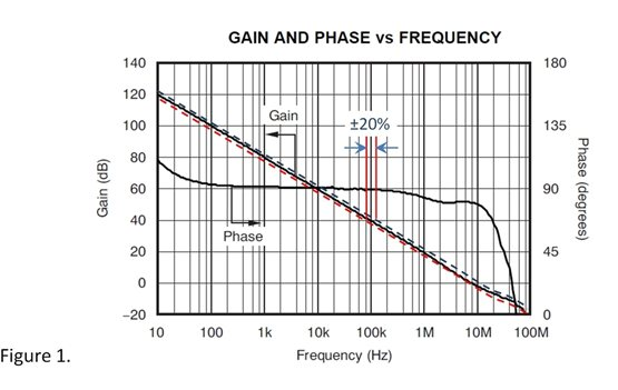
Bandwidth—The gain-bandwidth product (GBW) of an op amp is primarily controlled by the input stage current and the on-chip capacitance value. Changes in these two variables can produce a range of GBW variations of around ±20%. It seems that this is a wide range, but by choosing a large margin op amp, it is easier to make a wide range of GBW designs. If necessary, you can use some feedback components to control the closed-loop bandwidth of your application. Note that this change looks very small on the open loop gain/phase map (see Figure 1).

The slew rate is affected by the same variables such as bandwidth, internal current, and capacitance. In general, it is sufficient to choose an op amp that is 20% faster than the minimum demand speed. Perhaps you want to have more margin in some important applications. Most applications do not push the amplifier up to its conversion rate limit, so there is no problem with this.
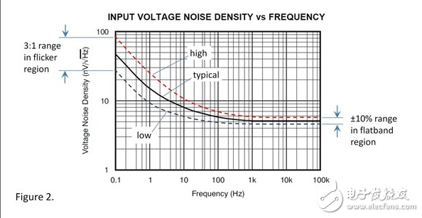
Voltage Noise - The amplifier's wideband or flatband voltage noise is primarily dependent on the current of one or more input stage transistors. Large currents reduce noise in a square root. So a 20% change in current can result in a flatband noise density change of about 10% (see Figure 2).

Low-frequency 1/f noise (also known as flicker noise) is another matter, and it varies more. The noise amplitude of the 1/f zone varies from approximately 3:1. The difference between JFET and CMOS fabrication processes may be slightly larger. This noise region determines the peak to peak noise level of the low frequency band (typically specified as 0.1 to 10 Hz).
There are indeed some good guidelines, but it is not possible to specify the exact range of changes in the amplifier design and the IC process used. However, some of the information is better than none, and most designs are well adapted to these estimated differences.
The margins that are right for your application may vary depending on the type of device you are designing (and possibly the end product test you are doing). The difference between the margin and the specification will affect the target margin for your design. This "engineering judgment" is an important factor in good analog design.
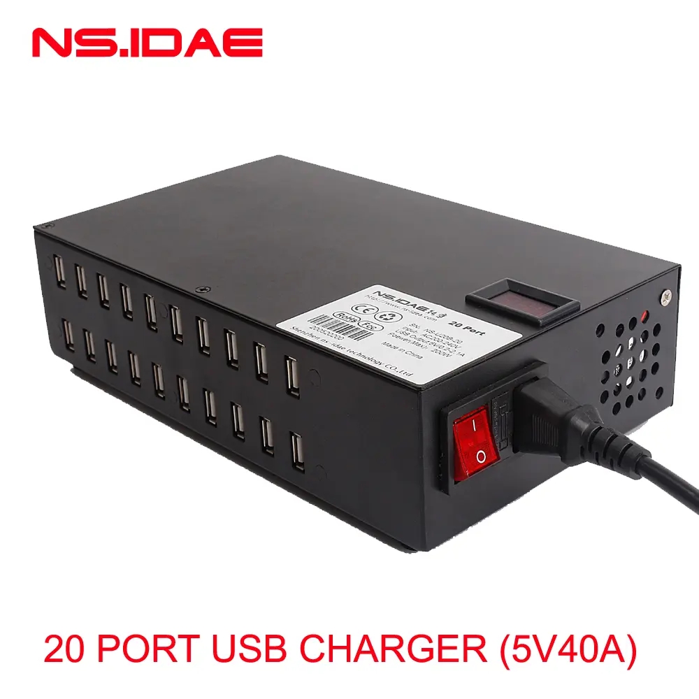
20 port USB charging station
This 20 port USB charging station has high quality patience and persistence. And the maximum demand that meets the charging is up to 20 devices. Each interface has an independent chip, which effectively prevents mutual interference between each port. Static single fan automatically heat dissipation to ensure the safety of the charging equipment. Provide overvoltage, short -circuit, overload, overload, temperature and voltage regulator protection.

20 Port Usb Charger,Usb Ai Smart Charger,20 Port Intelligent Charger,20 Port Electronic Devices Charge
shenzhen ns-idae technology co.,ltd , https://www.szbestchargers.com