On November 27, 1990, a company called Advanced RISC Machines (ARM) was established in Cambridge, England. The company, which was independent from the joint venture between Acorn and Apple Computer, launched the ARM7 architecture three years after its inception, indirectly driving the mobile phone boom of the 1990s and opening up a licensing approach focused on instruction sets and architecture.
Today, 25 years later, even the founders of ARM may not have thought that the company can achieve its current achievements. As of the third quarter of 2015, global shipments based on the ARM architecture exceeded 75 billion, and the ARM architecture is used in 85% of smart mobile devices, especially in the smart phones we are familiar with, 95% of devices use All are processors based on the ARM architecture.
These achievements are attributed to its thousands of partners and its unique business model. ARM's products are not chips, but semiconductor intellectual property (IP), providing ARM's advanced IP technology to chip companies or hardware system vendors through licensing models, and charging license fees from licensees. After obtaining these IPs, vendors can design and develop chips. And the relevant copyright tax will be delivered after shipment.
In the past, when embedded devices and mobile devices developed rapidly, ARM gained considerable profits and growth rates through its IP-licensed model with its high-quality design. In the current environment of the Internet of Things, ARM It is also savvy, cutting into new markets with new products, technologies and models, and the next wave of growth opportunities.
Mali-470 meeting the needs of the Internet of Things
Among ARM's rich IP products, GPU IP is an important part. According to ARM data, as of 2014, ARM Mali-based GPU chips shipped more than 550 million worldwide. These products are used in 75% of the numbers. TV, over 50% of Android tablets and over 35% of smartphones. In the face-to-face IoT market, ARM has introduced the GPU product Mali-470, which is designed specifically for the Internet of Things and the wearable market.
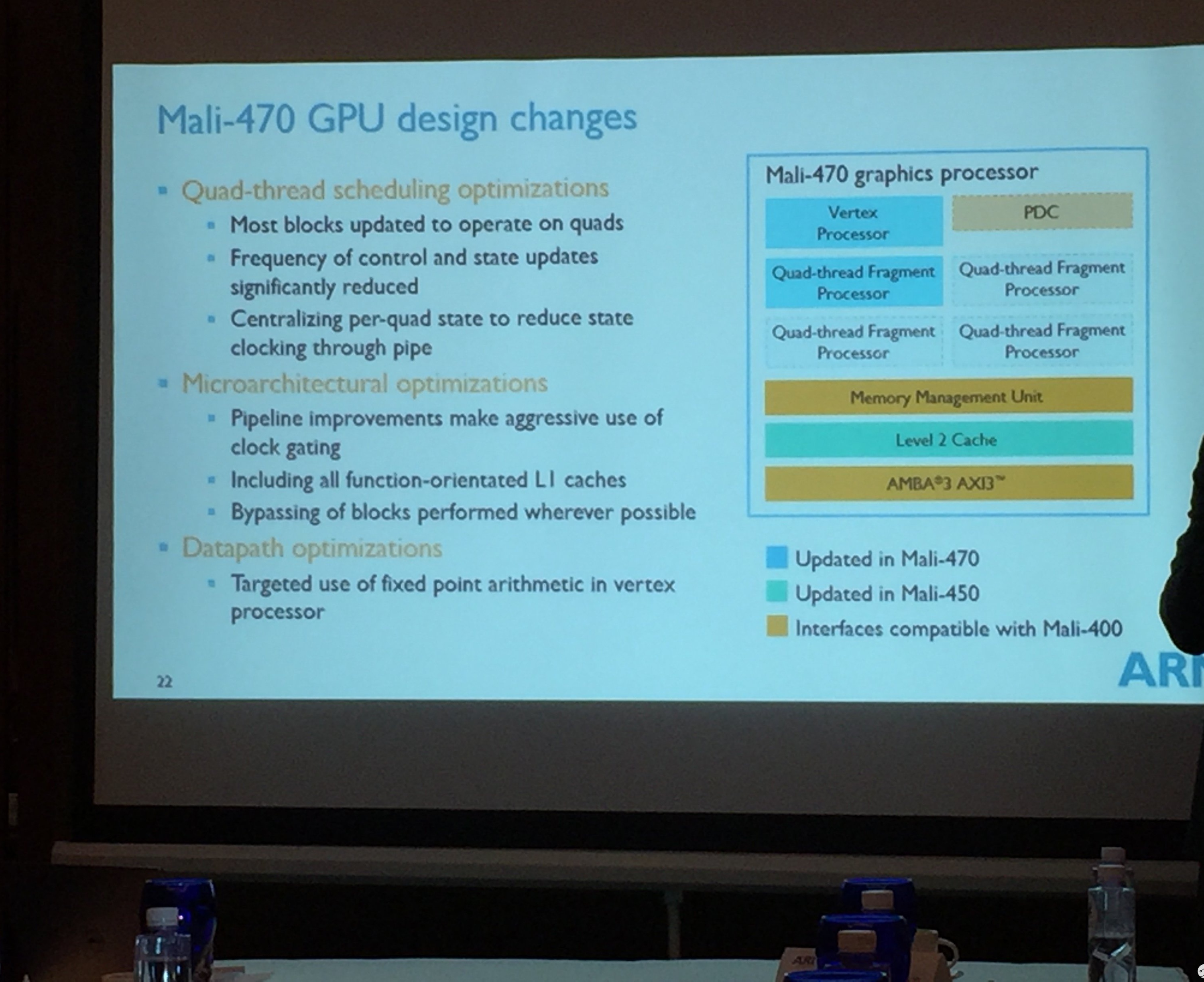
Mali-470 related parameters
According to Dennis Laudick, vice president of marketing for ARM Multimedia Processors, the Mali-470 is optimized for energy efficiency compared to the previous generation Mali-400, which consumes about half the power and doubles energy efficiency. . In addition, the Mali-470 optimizes energy efficiency for screen resolutions, with a single core configuration up to 640x640 screen resolution and multi-core configurations for higher resolutions, reducing screen cost while improving picture frame rate and improving overall instant response. . The chip size is 10% smaller than the Mali-400. This also makes it more suitable for devices that have limited battery capacity and heat dissipation, such as wearable devices. In terms of performance, the Mali-470 is maintained at the same level as the Mali-400, which means that its energy-saving improvement is not achieved at the expense of performance.
"At present, most Android, Android Wear and other emerging systems use the OpenGL ES2.0 API and driver stack, and OpenGL ES2.0 does allow the user interface to achieve an ideal balance between pixel control and energy efficiency. Therefore, the Mali-470 is also using the OpenGL ES2.0 standard," said Dennis Laudick.
The use of modern GPUs is generally designed with the CPU, and ARM is also a huge CPU and GPU IP vendor. What are the requirements for the matching of Mali-470 and CPU IP?
Dennis Laudick said the Mali-470 works with low-power chips on the same energy-efficient Cortex-A7 or A53 processor design. It also supports multiple combinations of one core to four core.
Under the premise of increasing wearable displays, the first device equipped with this GPU is expected to be launched at the end of 2016, which will be an important part of ARM's attack on the Internet of Things in the Internet of Things.
Cortex A35 processor based on ARMv8-A architecture
Before we introduce this new product, let's first understand what the architecture is. The so-called architecture is the "instruction set architecture", we usually say that ARMv8, ARMv7-A, ARMv6, etc. are some RISC instruction sets designed by ARM. The so-called instruction set architecture is a set of reduced instructions introduced by ARM. It is the lowest level command of the computer. For example, the application needs to read data from the memory, and finally the instruction is realized by calling the ARM design instruction. .
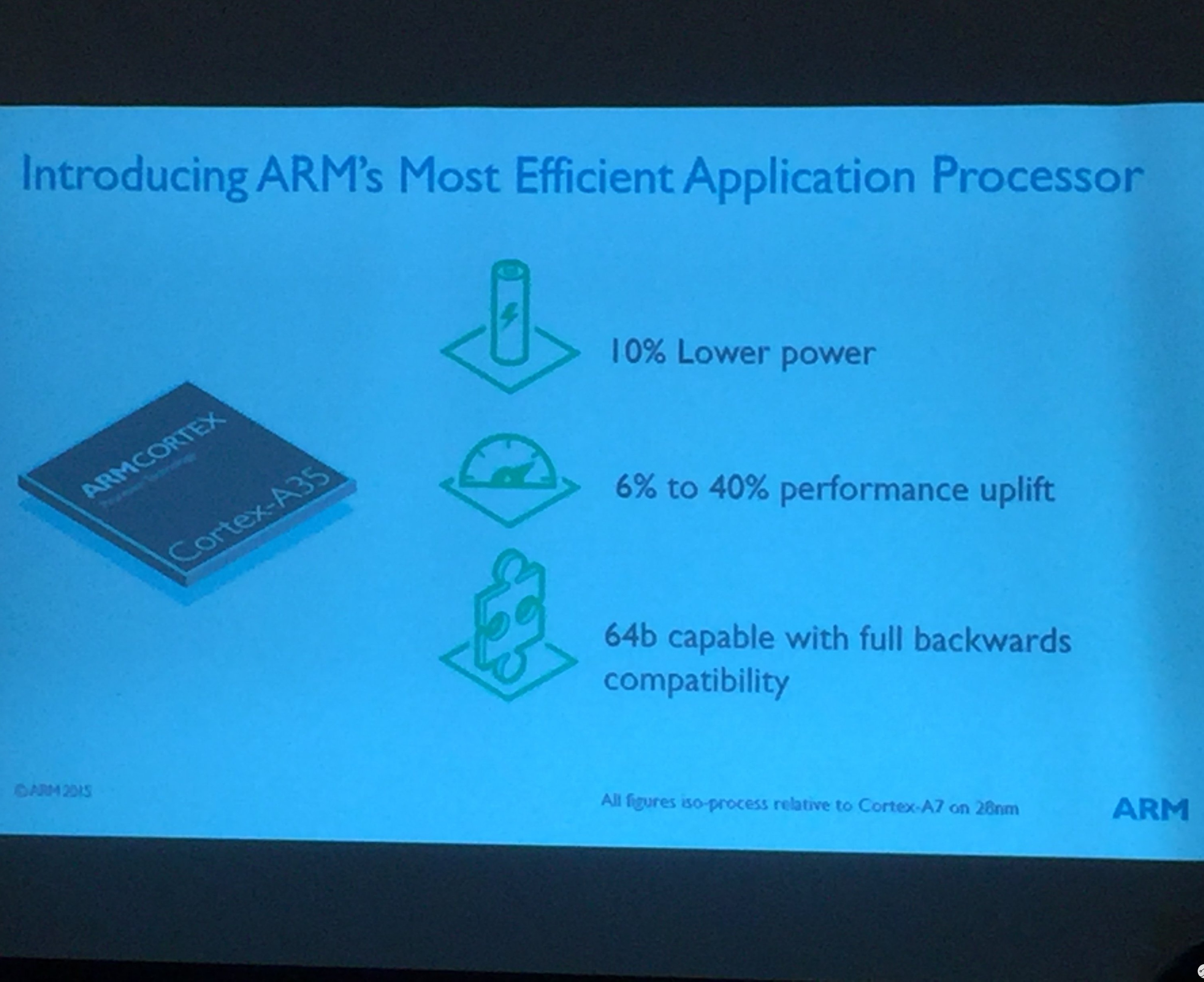
Cortex A35 basic introduction
ARM's latest ARM-v8-A architecture is the largest change in ARM architecture in the past 20 years. The new features such as ExecuTIon State, ExcepTIon Level, and Security State have broken through our traditional understanding of ARM architecture. The new architecture is also obvious for the improvement of the processor, the new Cortex A35 processor can fully reflect its characteristics.
According to Ian Smythe, director of marketing for the ARM processor division, the Cortex-A35 is the most energy-efficient processor ever built, with the software maturity and 64-bit computing performance of the ARMv8-A architecture. The target power consumption does not exceed 125 mW, and it has already achieved 90 mW in the 28 nm process and 1 GHz frequency. If you use the 16/14nm process, you can easily exceed 2GHz while keeping power consumption constant or even lower. But in general, manufacturers will focus on the 28nm process, because this is the best node for cost performance.
As the successor to the ARM Cortex-A7, the Cortex-A35 not only has the power level of the Cortex-A7 processor and ARM big.LITTLETM multi-core configurability, but also the software maturity and 64-bit computing of the ARMv8-A architecture. performance. ARM has better power consumption and performance, with an average performance and efficiency portion that can be increased by 20%.
Compared with the Cortex-A53, the Cortex-A35 can retain 80-100% performance, but the power consumption is reduced by 32%, the area is reduced by 25%, and the energy efficiency is increased by 25%. The Cortex-A35 can be combined with the Cortex-A53, Cortex-A57, Cortex-A72 and other cores to form a big.LITTLE hybrid architecture system to further enhance system energy efficiency.
These superior performance comes from its subtle design. The Cortex-A35 is similar in architecture to the Cortex-A53, Cortex-A7 or sequential limited dual-emission design, 8-stage pipeline, but has been carefully optimized to improve each module, even incorporating the A72. Some of the latest elements, performance and energy efficiency have been greatly improved.
Especially at the front end, the Cortex-A35 redesigned the instruction prefetch unit to improve the branch prediction accuracy, the instruction prefetch bandwidth is more balanced, and the instruction queue is smaller.
It also uses the Cortex-A53's cache and memory architecture. It can be configured with 8-64KB level 1 instruction and data cache, 128KB-1MB L2 cache, and NEON/FP unit. It improves storage performance and supports full pipeline double precision. Multiplication, also equipped with hardware retention status (independent power domain) for CPU core and NEON pipeline to improve power management efficiency.
The future mobile market will continue to grow. ARM has already conquered many developers with the Cortex-A7, and the new Cortex-A35, the world's most powerful 64-bit mobile processor, will bring consumers to the mobile and embedded markets. The advantage of 64-bit computing.
ARMv8-M architecture with TrustZone technology for device security
In the environment of various equipment explosions, especially in the current situation of the Internet of Everything, how to ensure the safety of equipment has become a concern of major semiconductor manufacturers and developers. ARM is the IP provider of semiconductor upstream, from the IP level. Get started and help developers solve security problems, all from their TrustZone technology. Before introducing TrustZone, we need to clarify a concept. The difference between the ARMv8-M architecture and the ARMv8-A architecture in the previous section is that the former is only for the development of the Cortex-M series and only supports 32 bits; the latter can Develop 32 or 64 bit Cortex-A processors.
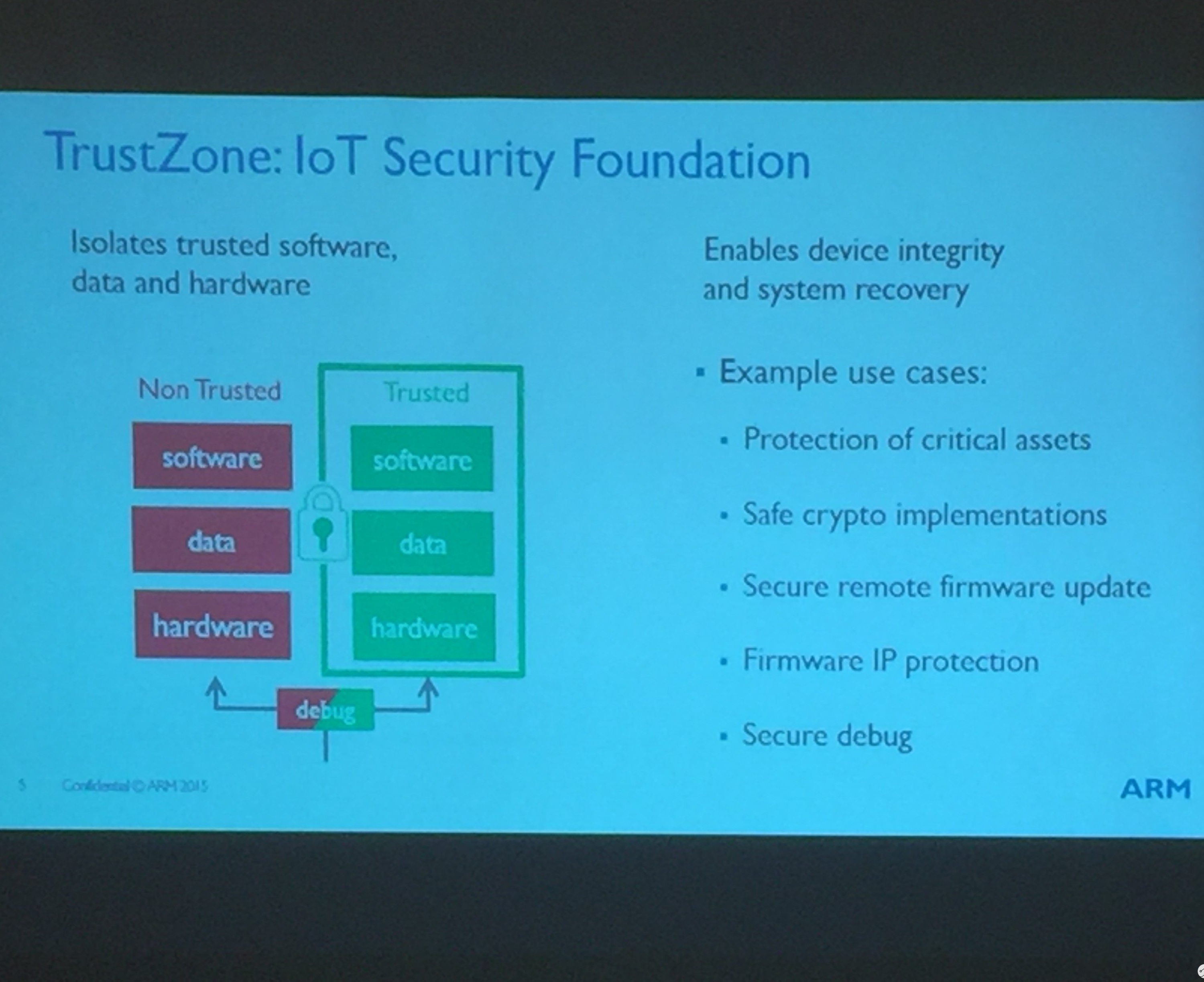
Introduction to TrustZone
Going back to TrustZone, this is ARM's architecture for consumer electronics security. We know that there are several forms of solutions for device security threats:
(1) External hardware security module
For example, the SIM card on the device. The advantage of this method is that the SIM card has specific hardware and software security features, can protect the resources such as keys in the card, and the cost of breaking the protection is very high. The disadvantage is that the communication speed with the interface of the device is low, and the security of the user interface cannot be protected, that is, the data that interacts with the user is safe, so the solution cannot provide good protection in terms of transaction payment;
(2) Internal hardware security module
That is, put the function similar to the smart card directly into the SoC. This method can only protect resources such as keys and cannot protect user interaction data. There are two cores in the SoC: a normal app core and a security core. The communication speed between the two cores will also be lower. Moreover, it is also very cautious in terms of occupying the SoC area, access control of the debug port, and the like;
(3) Software virtualization
If virtualization technology wants to protect the security of the user interface, it needs to add a lot of verification to the control of the GPU, which will have a great impact on the performance of graphics processing. At the same time, the debug port is still a problem.
ARM's TrustZone hardware architecture is an extension of the security system throughout the system design process, with the goal of preventing multiple specific threats to the device (note that this threat comes from malware, black workshops, and possibly from devices). Holder). The security of the system is obtained by dividing the hardware and software resources of the SoC into two worlds.
According to James McNiven, General Manager of ARM Processors: "ARM's TrustZone CryptoCell product line takes data protection to a new level. This enhanced security technology creates a hardware security add-on layer that enables isolated storage of high-value assets. Optimized encryption and lifecycle management of important information."
This new ARMv8-M architecture makes it easier and faster for developers to write code that covers the widest range of processors from ARMv8-M architecture, from the most energy efficient to the highest performance. It also makes it easier to integrate low-power ARM Cortex-M processors with the more powerful Cortex-A processors to develop higher performance system-on-chip (SoC) products. By enhancing the industry's ability to design high-end embedded SoCs, ARM brings more opportunities for smarter interconnect technologies. All areas where the analysis and use of safety data will bring new value will benefit from this, including health, identification or factory machine management.
As a complement to the ARMv8-M architecture, the ARM AMBA 5 AHB5 specification has been introduced to extend the TrustZone security foundation from the processor to the entire system of embedded design. The new AHB interconnect standard is now open for download, adding security controls and more memory types to meet the demands of higher performance embedded systems. AMBA 5 AHB5 supports ARMv8-M architecture and TrustZone technology.
One product solves the problems of security, scalability and developer efficiency that the IoT developers pay attention to in the future. It can be seen that ARM has worked hard on this product. And this kind of product that can isolate software and data, and can isolate hardware, is bound to be welcomed by the market.
Free Cortex-M0 processor IP
At the beginning of the article, we mentioned that ARM's profit model mainly relies on IP authorization, and its authorization mode is mainly divided into three types:
(1) Processor authorization
ARM designs a CPU or GPU and then licenses it to the partner. After you buy them, you can only implement them according to the drawings. There are not many places to play, but how to implement them is easy, such as which modules, several cores, how many caches, how high frequency, what crafts, who will be used. Work and so on.
ARM will also provide you with guidance and assistance, but how to turn the solution into a chip and set the specifications, it depends on you.
(2) Processor Optimization Package / Physical IP Package Authorization (POP)
If you want to be an ARM processor, but you have no limited strength, what should you do? ARM has carefully prepared a series of optimized processor design solutions, you can choose the right one for your own needs.
In this way, you can quickly produce the product at a low cost. Of course, the space that can be freely played is small. The processor type, foundry, and process are all well-defined. For example, the Cortex-A12 processor requires you to use it in TSMC. Produced in the 28nm HPM process, or in the 28-SLP process at Global Foundries.
(3) Architecture/instruction set authorization
If you are strong, you can only buy ARM architecture / instruction set (ARMv7, ARMv8), and then study the design chip yourself, Qualcomm Krait, Apple Swift is a typical representative.
These self-designed processors and ARM are instruction set compatible, but there is no direct comparability. For example, you can't say that Krait 400 and Cortex-A15 are better or worse. They are different implementations at the same level.
If you become an authorizer of ARM, there are two parts of money that must be paid: upfront license fee, royalty. There are many other charging items, such as software tools, technical support, and so on. The pre-authorization fee is generally $1 million, and more than $10 million (or possibly less or more), paid in one lump sum. How much depends on the complexity of the licensed technology purchased. The royalty is a point for each chip sold, usually 1-2% of the price.
These high licensing fees increase the chip's development threshold. During the period of high demand for IoT chips, the foundry and non-fab modes were very clear. Some of the ideas and creative chips are so expensive that they are stuck in the licensing fees and cannot implement the ideas. ARM has seen this and deliberately changed the licensing method of Cortex-M0 to help the Internet of Things market.
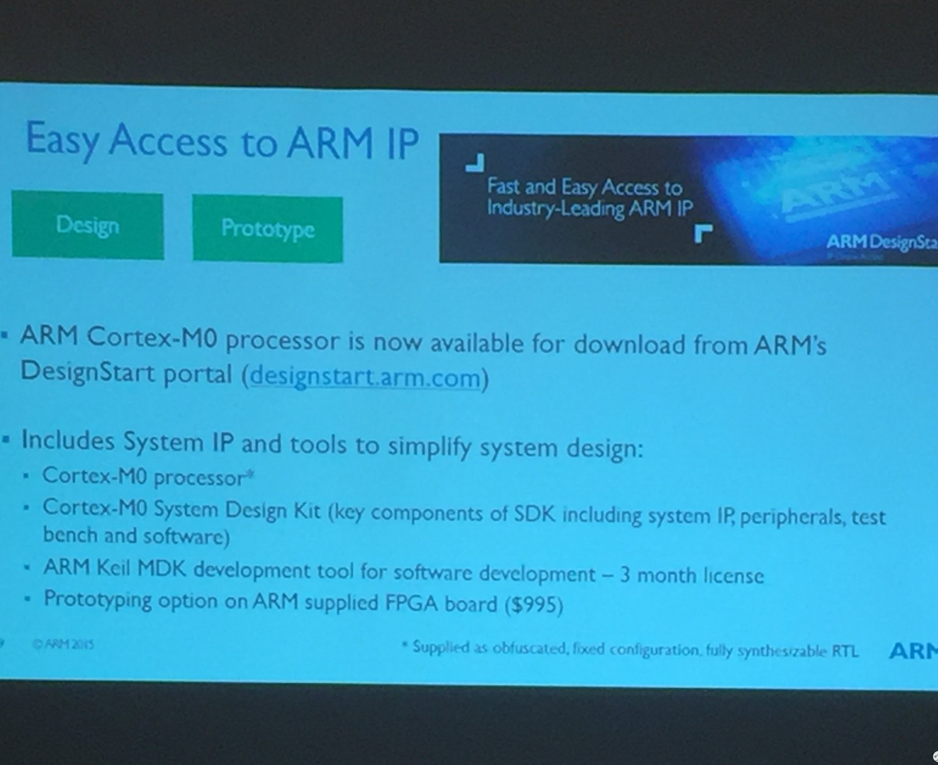
According to James McNiven, general manager of the ARM processor division, ARM will provide free Cortex-M0 processor IP to designers who design, prototype and manufacture SoC components prior to commercialization with the ARM Cortex-M0 processor. And low-cost FPGA prototyping.
“Designers can access this packaged service through the ARM DesignStart portal, including: Cortex-M0 processor and System Design Kit (SDK), including system IP, peripherals, test platforms, and related software; A 90-day free license for the ARM Keil® MDK development tool.†James McNiven added.
But this kind of authorization is not completely free.
James McNiven said that if developers want to commercialize their designs, they can purchase simplified, standardized, fast licenses for $40,000 to use the ARM Cortex-M0 processor-related IP, SDK, and Keli MDK development tools. For commercial purposes, technical support from ARM is also available. Of course, the copyright tax at the sales stage is also subject to payment.
Simplify the licensing model, lower the threshold, and allow more customized ICs to be market-oriented. This is a great blessing for developers. I hope that with the promotion of ARM, more chip vendors will emerge in China and the domestic semiconductor chip system will be expanded.
Mbed: ARM's weapon for the Internet of Things?
Nowadays, almost all semiconductor manufacturers must talk about the Internet of Things, and hardware developers are basically concerned about the Internet of Things. Everyone is so keen, mainly in the trillion-dollar market that the Internet of Things is brewing. In addition to using the processor to capture the market, ARM also hopes to use mbed to go to the Internet of Things.
mBed is ARM's suite of tools for the rapid development of ARM architecture microcontroller applications for the IoT market, including a free Software Development Kit (SDK), Hardware Development Kit (HDK) and Web-based The online compilation environment (mBed Compiler) three parts of the specific content.
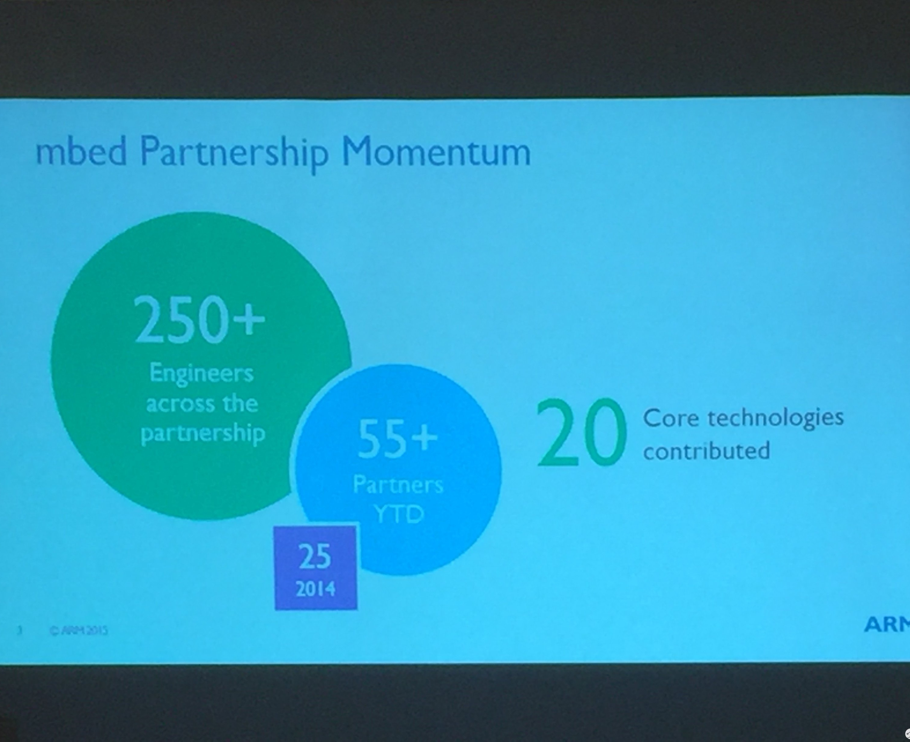
Increase in mbed partners
That is, ARM mbed firstly designs a hardware abstraction layer, shields different MCU vendors from providing the difference between micro-processing, and provides developers with a unified hardware abstraction layer; and then provides a hardware reference design, which is provided by HDK for user development. Unified program upload interface, single-step debugging interface, serial debugging interface, users can start software development without purchasing other hardware; at the same time, in order to save the trouble of user development environment installation, mbed provides a complete browser-based micro Processor software development environment, including code writing, program compilation, version control and other functions, users can develop as long as the Internet, the compilation results can be downloaded and saved to the mbed development board to work, very convenient.
In summary, mbed helps you build your own embedded connectivity devices quickly and easily, from planning to prototyping to production. Mbed can do this by allowing you to write software on an operating system (mbed operating system) that works with all mbed-enabled hardware, and the operating system can also connect to it using our mbed device connector service. cloud. In other words, the ARM mbed IoT device platform provides all the key components of IoT device development, creating secure and efficient IoT applications through ARM's mbed operating system, mbed device server, and mbed community ecosystem.
This platform has also achieved good results.
In 2014, only 60,000 developers used mbed for IoT product design, but in 2015 this figure rose to 150,000. The number of devices connected to the mbed development environment has also increased from 2.9 million last year to 4.3 million this year. The number of mbed partners has also risen from 25 in 2014 to over 55 this year.
However, ARM's idea of ​​unifying the Internet of Things through a platform is not known. We know that vendors such as Google, Huawei and Intel also hope to use the OS to integrate the Internet of Things platform. Is ARM going to unify these standards, or to let more competitors compete in the market and try to win over their customers. These methods are not yet judged, but ARM is the main supplier of the device core. In either case, the business in this field will only increase.
From these products, we can see that ARM is bound to win the future of the Internet of Things. The consolidation of traditional products is also a matter of course. It seems that Intel wants to take away the Internet of Things pie from ARM and it will take some extra effort.
Copper Clad Steel ,Copper Clad Steel Highly Conductive,Copper Clad Steel Strand,Anti-Oxidation Copper-Clad Stee
changzhou yuzisenhan electronic co.,ltd , https://www.yzshelectronics.com