In the electronic design, after the project schematic design is compiled and passed, the PCB design is needed. PCB design First, after determining the dimensions of the board, the design of the stack, and the overall concept of partitioning, the first step in the design process is the layout of the components. The various components are placed in its proper position. The layout is a crucial link. The good or bad layout results directly affect the effect of the wiring, thus affecting the entire design function. Therefore, a reasonable and effective layout is the first step in the success of PCB design.
Before the PCB layout, the circuit is partitioned by module according to the entire function. In the regional planning, the analog part and the digital part are isolated according to the function, and the high-frequency circuit is isolated from the low-frequency circuit. After the partition is completed, the key elements in each area are considered, and other elements in the area are placed in the right places with the key elements as the focus. When placing components, consider the internal circuit traces between the subsystem circuits, especially the timing and oscillator circuits. In order to remove the potential problems of electromagnetic interference, the placement and layout of the components should be systematically inspected to facilitate wiring, reduce electromagnetic interference, and make the appearance as satisfying as possible.
Common PCB layout problems and confusion
The success of a product, on the one hand, requires a good quality of function, on the other hand requires beauty, layout your circuit board as a craft. There are often questions and concerns about the layout of PCB components.
PCB shape and machine match? Is the spacing between the components reasonable, and is there a level or height conflict?
Whether the PCB needs to be imposed, whether to reserve the edge of the process, whether to reserve the mounting holes, and how to align the positioning holes?
How to consider impedance control, signal integrity, power signal stability, power module cooling?
Is it necessary to replace the components that need to be replaced frequently, and can the adjustable components be easily adjusted?
Is there any distance between the thermal element and the heating element?
The entire board EMC performance, how to layout can effectively enhance the anti-jamming capability?
Excellent layout principles of PCB components
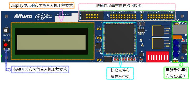
Divide the area first. According to the functional unit of the circuit, consider all the components of the circuit as a whole, and divide each functional circuit unit into general areas according to the module, so that the layout is suitable for signal circulation, and the direction is consistent as far as possible.
As shown in the above figure, the general functional modules such as the power supply section, the core control section, the signal input processing section, the signal output processing section, the connector section, the human-computer interaction section, and the like. Divide the module area according to the actual functional requirements of the circuit board. The general principle is that the power section is centrally located on the edge of the board, the core control section is in the middle of the board, the signal input section is on the left side of the core control section, and the signal output section is on the right side of the core control section. The connector part is arranged on the edge of the board as much as possible, and the human-computer interaction part must take into consideration the requirements of ergonomics for reasonable layout. Under the premise of guaranteeing the electrical performance, the components of each functional module should be placed on the grid and arranged parallel or perpendicular to each other, in order to be neat and beautiful.
Then center around the core components of each functional module circuit and lay out around this center. The components should be evenly, integrally, and compactly arranged on the PCB. Minimize and shorten the leads and connections between the components to facilitate wiring and reduce electromagnetic interference. In PCBs, special components such as power devices, tunable devices, heat-generating and heat-sensitive devices, key components in high-frequency parts, core chips, components susceptible to interference, devices with large or heavy weights, high voltage devices, and some The position of these different components needs to be carefully analyzed. The layout must meet the requirements of circuit functions and production requirements. Inappropriate layout may cause circuit compatibility issues, signal integrity issues, leading to PCB design failure. When the layout of special components is laid out, the following principles must be observed:
DC/DC converters, switching elements, and rectifiers should be placed as close to the transformer as possible, with rectifier diodes as close as possible to the voltage regulator components and filter capacitors. To reduce the length of its line.
The EMI filter should be as close to the EMI source as possible. Minimize the connections between high-frequency components and try to reduce their distribution parameters and electromagnetic interference between them. Components that are subject to interference should not be too close to one another, and the input and output should be as far apart as possible.
For the layout of potentiometers, adjustable inductors, variable capacitors, microswitches and other adjustable components should consider the structure requirements of the whole wrench, some often used switches, in the structure allows, it should be easy to place Place of contact. The layout of components is balanced and dense.
The heating element should be placed on the edge of the PCB for heat dissipation. If the PCB is mounted vertically, the heating element should be placed above the PCB. The thermal element should be away from the heating element.
In the layout of the power supply, try to make the layout of the device easier for the power cable routing. Consider reducing the area of ​​the input power circuit during layout. When the circulation is satisfied, the input power line is prevented from running over the board, and the looped area is too large. The power line and the ground line are well matched to reduce the influence of electromagnetic interference. If the power cord and ground wire are not properly matched, many loops may occur and noise may be generated.
Because of the different frequencies, high- and low-frequency circuits have different methods of interference and interference suppression. Therefore, in the layout of components, digital circuits, analog circuits, and power circuits should be arranged separately according to modules. The high-frequency circuit and the low-frequency circuit are effectively isolated, or divided into small sub-circuit module boards, with connectors connected between them.
In addition, special attention should also be paid to the distribution of strong and weak signals and the direction of signal transmission in the layout. To minimize interference, the analog and digital sections are separated and the high, medium, and low-speed logic circuits are maintained on the PCB. The PCB is partitioned by frequency and current switching characteristics. Noise and non-noise components are a little further away. The thermal element is far away from the heating element. The low-level signal path is far from the high-level signal path and the unfiltered power line. Separate analog and digital circuits from low levels to avoid common impedance coupling between analog circuits, digital circuits, and the power supply common return.
Smart PCB component layout case sharing
EMC considers: bypass or decoupling capacitors enhance stability and reduce interference
In PCB design, both analog and digital devices require this type of capacitor. Connect the bypass capacitor near its power supply pin. This capacitor is usually 0.1uF. The layout requires pins as short as possible, and as close as possible to the device to reduce the inductance of the traces.
Bypass capacitors are commonly used in analog circuit designs to bypass high-frequency signals on power supplies. In general, the frequency of these high frequency signals exceeds the analog device's ability to reject high frequency signals. If bypass capacitors are not used, noise may be introduced into the signal path, and even more serious conditions may cause vibration and false response.
Digital Circuit Design Digital devices such as controllers and processors also require decoupling capacitors. One of the functions of this capacitor is to act as a "micro" charge reservoir. Because the digital circuit usually requires a large amount of current when performing a gate state switching or switching, the transient current generated during switching, if there is not enough charge when the switching action is performed, will cause a great change in the power supply voltage. Too large a voltage change will cause the digital signal level to go into an unstable state, which may cause the status of the digital device to be mis-executed. Therefore, it is a good practice to add bypass or decoupling capacitors at the power supply pins or power pins of digital devices.
The most sensitive signals in a microcontroller-based (MCU)-based system are the timing, reset, and interrupt signals. Oscillators are especially sensitive when switching. These circuits cannot be paralleled with high current traces to avoid signal interference and misjudgment. Oscillators or ceramic resonant clocks are RF circuits that must be effectively laid out to the nearest distance and the traces must be the shortest to reduce their sensitivity. The following figure uses DIP-packaged oscillators or ceramic resonators as an example. The oscillation circuit should be placed as close to the microcontroller as possible, with symmetrical positions so that the trace distance is the shortest. The ground of the oscillating circuit should be connected to the grounding pin that may use the shortest path. The power and ground pins should be connected directly to the power supply section of the PCB.

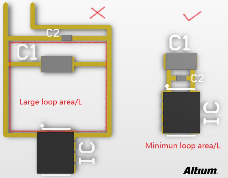
Similarly, when a logic switch on a circuit board generates a transient derivative current on the power line, the inductance of the power line can be reduced through multiple layers of printed circuit boards (power planes) because the power lines are somewhat inductive. Use slower logic to lower the switching speed. However, the former increases costs, and the latter reduces the performance of the system. In this case, the power line's communication interference can be reduced by the decoupling capacitor. The decoupling capacitors (also known as sharpened capacitors) on the PCB for the digital chip should be placed as close to the chip's power pins as possible to minimize the trace distance and minimize the loop area. The left picture below shows an unreasonable decoupling capacitor layout that should be laid out like the right picture.
     Â
    2. 3D Device Check Avoid Conflicts - Connectors
In the PCB layout, it is not possible to see in real time how the real components are placed on top, including the volume and height of the components. Whether the whole circuit board is matched with the enclosure, whether the components inside the circuit board are in conflict with each other in the horizontal direction, and the installation cannot be completed. The most terrible thing is whether the height of the components is appropriate and there will be conflicts with the housing. This requires real-time realistic simulation and presentation in 3D to find problems early. To ensure that the circuit board and the shape of the shell match, height match, matching mounting holes.
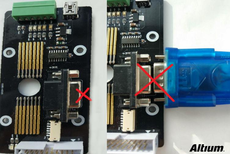
The layout of the connector on the PCB board is also crucial, and the layout of the good connector must take into account the convenience of future plug-in connections. Generally speaking, the connector needs to be close to the edge of the board and the interface is out of the board. It must not be too close to the board, so that the plug at the end of the connection line is blocked by the edge of the PCB and cannot be inserted. The unreasonable connector layout of the DB9 serial port as shown below causes the cable connector to fail to connect.
  Â
For the failure of this connector, if you can find the problem intuitively through the 3D view before doing PCB board, and modify it in time, it will save a lot of unnecessary time and effort. Instead of doing a good job of PCB board mounting and attaching devices, problems are discovered at the end of the connection.
3. Grid application: Place components round
Not long ago, an electronic industry colleague chatted with me and he wanted to place LED lights in a standard circular shape, keeping the same spacing. Said that in the process of placement is very nerve-racking, there is always no guarantee of a precise circular position, and the spacing is also difficult to calculate. I don't know which tool can easily implement this idea. To be honest, I hadn't tried this kind of placement, but I suddenly remembered that the AlTIum Designer had the ability to set up a polar grid. There were several other raster forms. Use this polar coordinate grid to try it out. Don't try, don't know, try a shock. With this fan-shaped grid, it is very easy to place LED components on a PCB in a circle! As shown below.
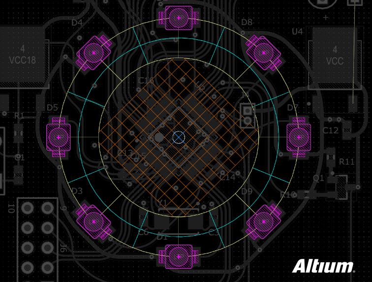
In this board, an ARM7 microprocessor is placed in the center of the board and placed at an angle of 45°. Then, using the center of the chip as the origin, set a regular rectangular grid with an inclination of 45°.
In the outer ring, there is another polar-coordinated fan-shaped grid, so that the LEDs surround a circle, and the LEDs arranged on this grid are accurate and delicate. At the same time when the component is placed, the mouse cursor automatically captures the grid points, positioning is precise, and the operation is extremely simple.
Whether in schematic design or PCB design, using grids to place target objects makes the drawings you design very clean, clean, and organized. In the PCB design, multiple grid combination applications are used when placing components. You can place the component to the desired location as you wish. This design magician you can think of, it can help you achieve. This is a wonderful and valuable feeling for engineers who dreary every day! The following figure shows the bare board view of the front and back sides of the design project PCB in 3D.
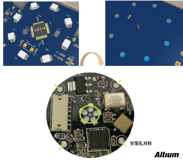
The circular PCB board above is another case of clever use of a grid. The five central mounting holes of the green circle are symmetrically distributed around the center point. The board is exactly symmetric along the four mounting holes.
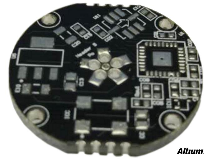
The following figure shows the PCB bare board. There are 4 half holes arranged on both sides of the plate. For board-to-board installation, the board is mounted as a modular device to the motherboard.
The material of this product is PC+ABS. All condition of our product is 100% brand new. OEM and ODM are avaliable of our products for your need. We also can produce the goods according to your specific requirement.
Our products built with input/output overvoltage protection, input/output overcurrent protection, over temperature protection, over power protection and short circuit protection. You can send more details of this product, so that we can offer best service to you!
Led Adapter,Mini Led Adapter,Security Led Adapter,Waterproof Led Adapter
Shenzhen Waweis Technology Co., Ltd. , https://www.laptopsasdapter.com