With the continuous development of GNSS (Global NavigaTIon Satellite System) and the accelerated construction of China's Beidou second-generation satellite navigation system, the application of satellite navigation and positioning system in various fields will be more extensive and deeper, with lower power consumption, lower noise and lower. The cost of satellite receiver chips has become a hot topic in current research, and as a mixer for spectrum shifting in RF front-end circuits, it is a very important module.
The ultimate goal of this paper is to obtain a low noise mixer for wideband applications suitable for GNSS receivers.
The purpose of this mixer design is to implement a low noise mixer for wideband applications with bandwidths covering all frequency bands (1 GHz to 1.6 GHz) of GNSS. The required specifications are as follows: 1) Input RF frequency: 1 ~1.6GHz; 2) IF output frequency: 46MHz; 3) RF power: -120~-30dBm; 4) Local oscillator power: -10dBm; 5) Operating voltage: 3.3V; 6) Conversion gain: 10dB; Noise figure: 4dB; 8) 1dB compression point: -17dBm.
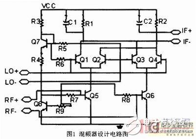
2 The overall design of the mixerThe circuit design of the mixer is shown in Figure 1.

The load circuit consists of R1, C1, R2, and C2, which form two RC first-order low-pass filters for filtering high-frequency signals such as LO and RF that leak to the output port of the mixer.
At the transconductance stage, Q8, R9 and Q5, R7 and Q8, R9 and Q6, R8 form a proportional mirror current source circuit. Among them, the base resistors R7 and R8 must be large enough to ensure that the RF signal power is well injected into Q5 and Q6, while preventing the interfering signal from crosstalking the RF signal from the base resistor. However, the base resistance should not be too large, otherwise the base current across the conduit will be too small, affecting the operating point, resulting in a decrease in gain. Since the input is a differential signal, R7 and R8 are required to be equal, and Q5 and Q6 are the same size.
In the switching stage, Q7 is connected in the form of a diode, which provides a bias voltage to the switching transistor. Q1 to Q4 are identical transistors. The base resistors R5 and R6 are also identical, and the resistance is required to be large enough to make the local oscillator signal. The power is effectively injected into the switch tube. R4 and R3 are used to set the magnitude of the bias current and the bias voltage of the switch stage, respectively. These two can not be too large, otherwise the branch current is small, which affects the setting of the cross-conduit operating point and flexibly adjusts the ratio of the two. Can make the voltage distribution more reasonable. In the circuit, the capacitance values ​​of C1 and C2 are 2pF; the bias transistors Q7 and Q8 select tubes with smaller sizes to save power. Their models are N05005011SH. The values ​​of the individual resistors are shown in Table 1.

In the analysis of gain and noise, we used the "MixConvGainNF SchemaTIc Template" environment provided by ADS for simulation. When the input RF signal frequency is 1.575GHz, the power is -85dBm, the output intermediate frequency is 46MHz, and the input local oscillator signal power is -10dBm, the measured conversion gain (conversiongain) is 15.79dB, and the single sideband noise figure is 4dB. as shown in picture 2.
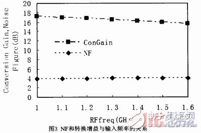
The design mixer is applied to a GNSS receiver, which requires receiving a radio frequency signal ranging from 1 to 1.6 GHz. The mixer also requires a higher gain and a lower noise figure in this range. Figure 3 shows the gain and noise over this range of variation, which is multi-point tested and then traced.

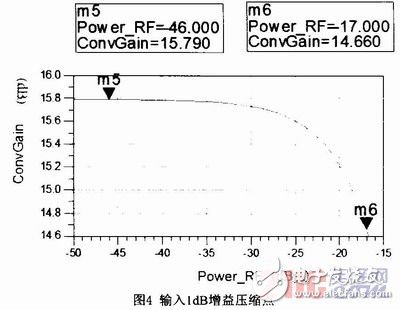
In addition, linearity is also an important issue to be considered by the mixer. Generally, the power of the GNSS RF signal received from the antenna is between -110 and -55 dBm. After being amplified by the low noise amplifier, the power of the RF signal input to the mixer is between -100 and -40 dBm. We know that when the input signal power becomes larger, the mixer will experience gain compression. Figure 4 shows the simulation results of the 1dB gain compression point of the mixer.

According to the simulation results in Fig. 3, it can be seen that in the 600MHz bandwidth range from 1 to 1.6 GHz, the gain is reduced by less than 2 dB, both being greater than 15 dB, providing sufficient gain to meet the gain design requirements. In addition, the noise figure also shows a small range of changes, achieving broadband low noise, in line with design requirements. According to the simulation in Figure 4, the 1dB gain compression point of the mixer is -17dBm, the linear range meets the application requirements, and also meets the project design requirements.
Gas Generating Set,Stable Performance Gas Generator,Gas Generating Set,Continuous Running Generator
Shaoxing AnFu Energy Equipment Co.Ltd , https://www.sxanfu.com