Diode is the simplest of the discrete components in the semiconductor family. Its most obvious property is its unidirectional conductivity, which means that current can only pass from one side but not from the other ( Flow from the positive electrode to the negative electrode). This article from the classification, naming methods of diodes, to the characteristics and selection of common diodes. It is also the basis of analog circuits, the first lesson.
First, the basics
1, the classification of diodes
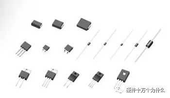
There are many types of diodes. According to the semiconductor materials used, they can be divided into germanium diodes (Ge tubes) and silicon diodes (Si tubes). According to the die structure, they can be divided into point contact diodes, surface contact diodes and planar types. diode.
According to the different uses of diodes, it can be divided into detector diodes, rectifier diodes, Zener diodes, switching diodes, Schottky diodes, LEDs and so on.
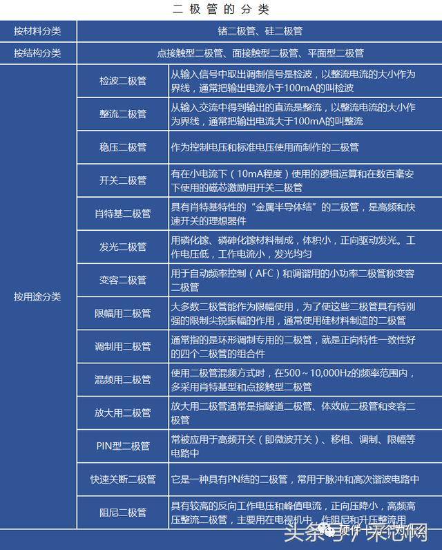
(Note: The above picture is taken from the core network)
2, the model name of the diode
(1) According to the domestic semiconductor device model naming method: the model name of the diode consists of five parts: main name, material and polarity, category, serial number and specification number (grade of the same product).
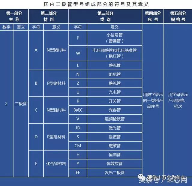
(2) The Japanese semiconductor device naming model consists of the following five parts:
The first part: the number and type of semiconductor devices are represented by numbers; "1" means a diode and "2" means a triode.
Part II: Use "S" to indicate a semiconductor device that has been registered with the Japan Electronics Industry Association;
Part III: The letter indicates the material, polarity and type of the device used;
Part IV: indicates the registration number of the device at the Japan Electronics Industry Association;
Part 5: Representing an improved product of the same model.
3, several common diode characteristics
(1) Rectifier diode
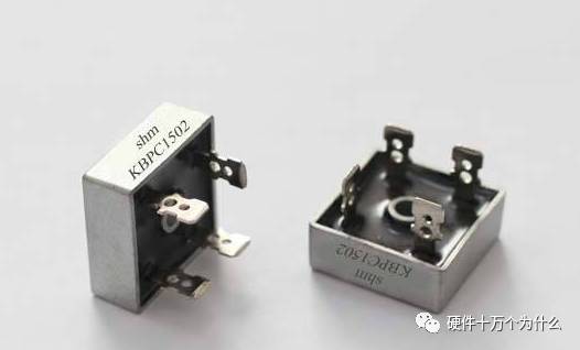
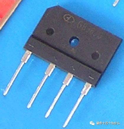
A diode that rectifies an AC power source into a DC current is called a rectifier diode. Since the junction capacitance is large, the operating frequency is low.
Typically, diodes with an IF of 1 amp or more are packaged in a metal case for heat dissipation; IFs are packaged in a full plastic package below 1 amp.
(2) Switching diode
In pulse digital circuits, the diodes used to turn the circuit on and off are called switching diodes, which are characterized by short reverse recovery times and can meet the needs of high frequency and ultra high frequency applications.
Switching diodes are available in contact type, planar type and diffused surface type. Generally, silicon switching diodes with IF<500 mA are mostly sealed with epoxy resin and ceramic chip package.
(3) Zener diode
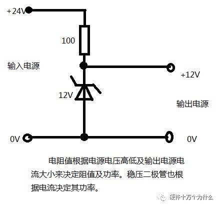
The Zener diode is a surface-bonded crystal diode made of silicon material. Because it can regulate the voltage in the circuit, it is called a Zener diode.
It is characterized by the fact that the voltage at the time of reverse breakdown of the PN junction does not change substantially with the change of current to achieve the purpose of voltage regulation.
(4) Varactor diode
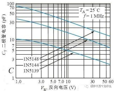
The varactor diode is a nonlinear capacitive element made by utilizing the characteristic that the capacitance of the PN junction changes with an applied bias voltage, and is widely used in microwave circuits such as parametric amplifiers, electronic tuning, and frequency multipliers.
Varactor diodes mainly emphasize the nonlinear relationship between capacitance and voltage through a series of methods such as structural design and process, and improve the Q value to suit the application.

(5) TVS diode
The TVS diode (Transient Voltage Suppresser) is connected in parallel with the protected circuit. When the transient voltage exceeds the normal operating voltage of the circuit, the diode avalanches, providing a path for the transient current to protect the internal circuit from excess voltage. The breakdown or overheating of the excess current burned.
Due to the large junction area of ​​the TVS diode, it has the advantage of escaping transient high current and has ideal protection.
Second, the choice of diode parameters
(1) rated forward operating current
The rated forward operating current is the maximum forward current value that the diode is allowed to pass during long-term continuous operation.
(2) Maximum inrush current
The maximum inrush current is the excess forward current that is allowed to flow. It is not a normal current, but an instantaneous current. Its value is usually about 20 times the rated forward operating current.
(3) highest reverse operating voltage
When the reverse operating voltage applied across the diode is high enough, the tube will break down and lose its unidirectional conductivity. In order to ensure safe use, the highest reverse operating voltage is specified. For example, the reverse withstand voltage of the lN4001 diode is 50V, and the reverse withstand voltage of the lN4007 is 1000V.
(4) Reverse current
Reverse current refers to the reverse current flowing through the diode under the specified temperature and the highest reverse voltage of the diode. The smaller the reverse current, the better the unidirectional conductivity of the tube.
The reverse current is closely related to the temperature, and the reverse current is doubled for every 10 °C increase in temperature.
Silicon diodes have better stability at high temperatures than germanium diodes.
(5) Reverse recovery time
When changing from the forward voltage to the reverse voltage, the current is generally not instantaneously cut off, and it is delayed for a little time. This time is the reverse recovery time. It directly affects the switching speed of the diode.
(6) Maximum power
The maximum power is the voltage applied across the diode multiplied by the current flowing through it. This limit parameter is special for Zener diodes and the like.
(7) Frequency characteristics
Due to the presence of junction capacitance, when the frequency is high to some extent, the capacitive reactance is so small that the PN junction is shorted. This causes the diode to lose its unidirectional conductivity and cannot work. The larger the PN junction area, the larger the junction capacitance and the lower the operation at high frequencies.
2, the choice of different diodes
(1) Detecting diode
The detection diode can generally be selected with a point contact type germanium diode. When selecting, the detection diode with high operating frequency, small reverse current and sufficient forward current should be selected according to the specific requirements of the circuit.
(2) Rectifier diode
Rectifier diodes are typically planar silicon diodes used in a variety of power rectifier circuits. When using a rectifier diode, the parameters such as maximum rectification current, maximum reverse operating current, cutoff frequency, and reverse recovery time should be considered. The rectifier diode used in the ordinary series stabilized power supply circuit has low requirements on the reverse recovery time of the cutoff frequency. As long as the maximum rectified current and the maximum reverse operating current meet the requirements of the rectifier diode according to the requirements of the circuit.
(3) Zener diode
The Zener diode is generally used as a reference voltage source in a regulated power supply or as a protection diode in an overvoltage protection circuit. The selected Zener diode should meet the requirements of the main parameters in the application circuit. The stable voltage of the Zener diode should be the same as the reference voltage of the application circuit. The maximum stable current of the Zener diode should be higher than the maximum load current of the application circuit by about 50%.
(4) Switching diode
Switching diodes are mainly used in household appliances and electronic equipment such as tape recorders, televisions, and DVD players, such as switching circuits, detection circuits, and high-frequency pulse rectifier circuits.
The medium speed switching circuit and the detection circuit can be selected from the 2AK series common switching diodes. High-speed switching circuits can be selected from RLS series, 1SS series, 1N series, 2CK series high-speed switching diodes.
The specific model of the switching diode is selected according to the main parameters of the application circuit (such as forward current, maximum reverse voltage, reverse recovery time, etc.).
(5) varactor diode
When selecting a varactor, consider whether the operating frequency, the highest reverse operating voltage, the maximum forward current, and the zero-bias junction capacitance are in compliance with the requirements of the application circuit. The junction capacitance should be changed greatly, the high Q value, and the reverse A varactor diode with a small leakage current.
3, TVS diode selection
(1) Minimum breakdown voltage VBR and breakdown current IR. VBR is the minimum breakdown voltage of TVS. At 25 ° C, below this voltage TVS will not produce avalanche. When the TVS flows through the specified 1 mA current (IR), the voltage applied to the two poles of the TVS is its minimum breakdown voltage VBR. According to the degree of dispersion of TVS VBR and standard values, VBR can be divided into 5% and 10%. For 5% of VBR, VWM = 0.85 VBR; for 10% of VBR, V WM = 0.81 VBR. In order to meet the IEC61000-4-2 international standard, TVS diodes must be able to handle ESD strikes of at least 8kV (contact) and 15kV (air). Some semiconductor manufacturers use higher impact standards on their products. For some portable device applications with special requirements, designers can select components as needed.
(2) Maximum reverse leakage current ID and rated reverse cut-off voltage VWM. VWM is the voltage that the diode can withstand under normal conditions. This voltage should be greater than or equal to the normal working voltage of the protected circuit. Otherwise, the diode will continuously cut off the loop voltage; but it needs to be as close as possible to the normal working voltage of the protected circuit. It is not going to face the overvoltage threat to the entire circuit before the TVS works. When this rated reverse cut-off voltage VWM is applied between the two poles of the TVS, it is in a reverse cut-off state, and the current flowing through it should be less than or equal to its maximum reverse leakage current ID.
(3) Maximum clamp voltage VC and maximum peak pulse current I PP . When the pulse peak current IPP with a duration of 20 ms flows through the TVS, the maximum peak voltage appearing at both ends thereof is VC. VC and IPP reflect the surge suppression capability of TVS. The ratio of VC to VBR is called the clamping factor and is generally between 1.2 and 1.4. VC is the voltage supplied by the diode in the off state, that is, the voltage passing through the TVS in the ESD strike state, which cannot be greater than the endurable limit voltage of the protected circuit, or the component is in danger of being damaged.
(4) Pppm rated pulse power, which is based on the maximum cutoff voltage and the peak pulse current at this time. For handheld devices, a 500W TVS is generally sufficient. The maximum peak pulse power consumption PM is the maximum peak pulse power consumption value that the TVS can withstand. At a certain maximum clamping voltage, the greater the power consumption PM, the greater the ability of the surge current to withstand. At a specific power consumption PM, the lower the clamp voltage VC, the greater the withstand current of the surge current. In addition, peak pulse power consumption is also related to pulse waveform, duration, and ambient temperature. Moreover, the transient pulses that TVS can withstand are not repeated, and the component-specified pulse repetition frequency (ratio of duration to pause time) is 0.01%. If a repetitive pulse occurs in the circuit, the accumulation of pulse power should be considered, possibly damaging the TVS.
(5) Capacitor amount C. The capacitor amount C is determined by the TVS avalanche junction profile and is measured at a specific 1 MHz frequency. The size of C is proportional to the current carrying capacity of the TVS tube, and C is too large to attenuate the signal. Therefore, C is an important parameter for the TVS of the data interface circuit. Capacitors For circuits with higher data/signal frequencies, the greater the interference of the diode's capacitors on the circuit, the noise or attenuation of the signal strength, so the capacitor range of the selected component needs to be determined based on the characteristics of the loop. The high-frequency circuit should generally choose capacitors as small as possible (such as SAC (500W, 50pF, ±10%), LCE (1.5KW, 100pF), low-capacitor TVS), and the circuit capacitors that require less capacitors can be selected to be higher than 40pF.
4, the difference between Schottky diode and ordinary diode
The initial conduction voltage drop of the silicon tube is about 0.5V, the normal conduction voltage drop is about 0.7V, and the conduction voltage drop is about 1V when the limit current is approached; the initial conduction voltage drop of the manifold is about 0.2V. The normal conduction voltage drop is about 0.3V. The conduction voltage drop is about 0.4V when the limit current is close. The initial conduction voltage drop of the Schottky diode is about 0.4V, and the normal conduction voltage drop is about 0.5V. The conduction voltage drop is about 0.8V when the limit current is approached.
Both diodes are unidirectional and can be used in rectification applications. The difference is that the normal silicon diode can withstand higher voltage, but its recovery speed is low, it can only be used in low frequency rectification. If it is high frequency, reverse leakage will occur because it cannot recover quickly, and finally the tube will be caused. Severe heat is burned; Schottky diodes have low withstand voltage, but they have a fast recovery speed and can be used in high frequency applications. Therefore, switching power supplies use this diode as a rectified output. However, rectification on the switching power supply The tube temperature is still very high.
The fast recovery diode refers to a diode with a short reverse recovery time (below 5 us). The process is mostly gold-doped. The structure has a PN junction structure, and some adopt an improved PIN structure. Its forward voltage drop is higher than that of ordinary diodes (1-2V), and the reverse withstand voltage is more than 1200V. From performance, it can be divided into two levels: fast recovery and ultra fast recovery. The former reverse recovery time is hundreds of nanoseconds or longer, while the latter is below 100 nanoseconds. Schottky diodes are diodes based on barriers formed by metal and semiconductor contacts, referred to as Schottky Barrier Diodes, with a forward voltage drop (0.4--0.5V) and a short reverse recovery time ( 10-40 nanoseconds), and the reverse leakage current is large, the withstand voltage is low, generally lower than 150V, and is mostly used in low voltage applications. These two types of tubes are commonly used for switching power supplies. The difference between the Schottky diode and the fast recovery diode is that the recovery time of the former is about one hundred times smaller than that of the latter, and the reverse recovery time of the former is about several nanoseconds~! The advantages of the former are low power consumption, high current, and ultra high speed. ~! Electrical characteristics are of course diodes ~! Fast recovery diodes in the manufacturing process using gold doping, simple diffusion and other processes, can obtain higher switching speed, but also get higher withstand voltage. Currently fast recovery diode The main application is to make rectifier components in the inverter power supply.
4, the difference between Schottky diode and fast recovery diode
Schottky diodes:
The reverse withstand voltage is low (generally less than 150V), the on-state voltage drop is 0.3-0.6V, and the reverse recovery time is less than 10nS. It is a "metal-semiconductor junction" diode with Schottky characteristics. Its forward starting voltage is lower.
In addition to the material, the metal layer may also be made of gold, molybdenum, nickel, titanium or the like. Its semiconductor material uses silicon or gallium arsenide, mostly N-type semiconductors. This device is electrically conductive by majority carriers, so its reverse saturation current is more conductive than minority carriers.
The PN junction is much larger. Since the minority carrier in the Schottky diode has a very small memory effect, its frequency response is only limited by the RC time constant. Therefore, it is an ideal device for high frequency and fast switching. It operates at frequencies up to 100 GHz. Also, MIS (Metal-Insulator-Semiconductor) Schottky diodes can be used to fabricate solar cells or light-emitting diodes.
Fast recovery diode: 0.8-1.1V forward voltage drop, 35-85nS reverse recovery time, fast switching between on and off, increasing the frequency of use of the device and improving the waveform. Fast recovery diodes are doped with gold in the manufacturing process, pure
Diffusion and other processes can achieve higher switching speeds, while also achieving higher withstand voltage.
At present, fast recovery diodes are mainly used as rectifying components in inverter power supplies.
 Â
Fast Recovery Diode (FRD) is a new type of semiconductor device that has been introduced in recent years. It has good switching characteristics, short reverse recovery time, large forward current, small size, and easy installation. Ultrafast Recovery Diode (SRD) is developed on the basis of fast recovery diodes. The reverse recovery time trr value is close to that of Schottky diodes. They can be widely used in switching power supplies, pulse width modulators (PWM), uninterruptible power supplies (UPS), AC motor variable frequency speed control (VVVF), high frequency heating and other devices, for high frequency, high current freewheeling diode or The rectifier is a promising power and electronic semiconductor device.
Schottky diodes: low reverse voltage values ​​(typically less than 150V), on-state voltage drop of 0.3-0.6V, and less than 10nS reverse recovery time. It is a "metal-semiconductor junction" diode with Schottky characteristics. Its forward starting voltage is lower. In addition to the material, the metal layer may also be made of gold, molybdenum, nickel, titanium or the like. Its semiconductor materials use silicon or gallium arsenide, mostly N-type semiconductors. This device is electrically conductive by majority carriers, so its reverse saturation current is much larger than that of a minority carrier-conducting PN junction. Since the minority carrier in the Schottky diode has a very small memory effect, its frequency response is only limited by the RC time constant, so it is an ideal device for high frequency and fast switching. It operates at frequencies up to 100 GHz. Also, MIS (Metal-Insulator-Semiconductor) Schottky diodes can be used to fabricate solar cells or light-emitting diodes.
Fast Recovery Diode: With a forward voltage drop of 0.8-1.1V and a reverse recovery time of 35-85nS, it quickly switches between on and off, increasing the frequency of use of the device and improving the waveform. Fast recovery diodes use gold doping, simple diffusion and other processes in the manufacturing process to obtain higher switching speeds and higher breakdown voltages. Currently, fast recovery diodes are mainly used in inverter power supplies for rectifying components. Fast Recovery Diode (FRD) is a new type of semiconductor device that has been introduced in recent years. It has good switching characteristics, short reverse recovery time, large forward current, small size, and easy installation. The Superfast Recovery Diode (SRD) is developed on the basis of a fast recovery diode. The reverse recovery time trr value is close to that of the Schottky diode. They can be widely used in switching power supplies, pulse width modulators (PWM), uninterruptible power supplies (UPS), AC motor variable frequency speed control (VVVF), high frequency heating and other devices, for high frequency, high current freewheeling diode or The rectifier is a promising power and electronic semiconductor device.
5, the difference between TVS diode and ESD protection diode
TVS transient voltage suppression here regardless of how TV is generated, such as direct or indirect lightning strikes, electrostatic discharge, large-capacity load switching and other factors caused by surges. Voltage from a few volts to tens of kilovolts or even higher. ESD The main applications of ESD protection are HBM and MM. Simply put, people or devices discharge (static) to the device, but the device cannot be damaged.
The typical HBM CLASS 1C model specifies a 100pF capacitor charging 1000V-2000V to discharge the device through a 1500 ohm resistor. The MM model is more energetic than the human body model. The capacitance is 200pF and the voltage is between 200-400, but There is no series resistance. Typical human body model discharge, peak current less than 0.75A, time 150ns typical machine model discharge, peak current less than 8A, time 5ns typical lightning surge (TVS used at power line entry) peak current 3000A, Time 20us
The principle of TVS diode and ESD protection diode is the same, but it is different according to power and package. Compared with TVS, ESD protection diode depends on those applications, such as ESD, which is mainly used for anti-static and anti-static. The required capacitance value is low, generally between 1--3.5PF is the best. TVS can not do this, TVS capacitance value is relatively high.
Laptop Stand Amazon Basics,Laptop Stand Amazon Basics Aluminum,Laptop Stand Amazon Basics Ventilated,Laptop Stand Amazon Choice,etc.
Shenzhen Chengrong Technology Co.ltd is a high-quality enterprise specializing in metal stamping and CNC production for 12 years. The company mainly aims at the R&D, production and sales of Notebook Laptop Stands and Mobile Phone Stands. From the mold design and processing to machining and product surface oxidation, spraying treatment etc ,integration can fully meet the various processing needs of customers. Have a complete and scientific quality management system, strength and product quality are recognized and trusted by the industry, to meet changing economic and social needs .
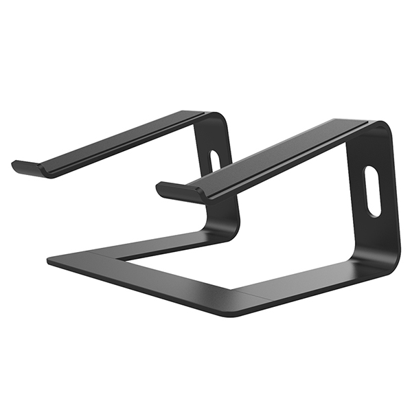
Laptop Stand Amazon Basics,Laptop Stand Amazon Basics Aluminum,Laptop Stand Amazon Basics Ventilated,Laptop Stand Amazon Choice
Shenzhen ChengRong Technology Co.,Ltd. , https://www.dglaptopstandsupplier.com