To understand the IO structure , first look at the role of pull-up and pull-down resistors.
First, pull-up resistor

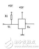
Pull-up is to clamp the indeterminate signal through a resistor at a high level! The resistor acts as a current limiting device at the same time! Pull down the same reason!
Pull-up resistors are used to provide current when the bus drive capability is insufficient. The general term is to draw current, and the pull-down resistor is used to sink current.
1. When driving a CMOS circuit with a TTL circuit, if the high level of TTL is lower than the high level threshold required by CMOS (1, TTL level: output high level > 2.4V, output low level <0.4 V. At room temperature, the general output high level is 3.5V, and the output low level is 0.2V. The minimum input high level and low level: input high level >=2.0V, input low level <=0.8V, The noise margin is 0.4 V. 2, CMOS level: 1 logic level voltage is close to the power supply voltage, 0 logic level is close to 0V, and has a wide noise margin.), then pull-up resistor is needed Increase the voltage value of the output high level.
2, OC gate must be added with a pull resistor before it can be used. (OC gate: the triode is called the open collector, the FET is called the open drain, referred to as the open drain output. With the "line and" capability, there is 0 to 0.)
3. In order to increase the driving ability of the output pin, the pin of the MCU is often connected to the pull-up resistor. (The AVR MCU can be configured to connect or pull up. 51 P1 P2 P3 are pulled up, P0 port is not used, so use P0 port to do the button, LCD and other applications should add their own pull-up resistor, otherwise you can not use the memory)
4, in order to prevent static damage on the CMOS chip, the unused pins can not be left floating, need to connect the pull-up resistor to reduce the input impedance, and provide a discharge path.
5, improve the ability of the bus to engage in electromagnetic interference, it is easy to electromagnetic interference when suspended.
Second, the choice of resistance of the pull-up resistor
1. In order to save power or make the sinking current large enough, the resistance value is large and the current is small.
2. To ensure sufficient drive current, the resistance is small and the current is large.
3. For high speed circuits, excessive pull-up resistors may cause the edges to become flat.
Based on the above three points, the pull-up resistance is generally selected as 1K-10K.
Third, the calculation of the pull-up resistance
When the OC gate outputs a high level, it is a high-impedance state. The pull-up current is provided by a pull-up resistor. The input terminal is not more than 100uA per port, and the output current of the output port is about 500uA. The standard operating voltage is 5V. The high and low thresholds are 0.8V (below this value is low); 2V (high threshold).
When the pull-up resistor is selected:
500uA x 8.4K= 4.2 When the output is greater than 8.4K, the output can be pulled down to 0.8V or less. This is the minimum resistance value, and it will not be pulled down. If the output current of the output port is large, the resistance value can be reduced, and it can be lower than 0.8V when the pull-down is performed.
When the output is high, the leakage current of the tube is ignored. The two input ports need 200uA.
200uA x15K=3V, that is, the pull-up resistor has a voltage drop of 3V, and the output port can reach 2V. This resistance value is the maximum resistance value, and then it will not reach 2V. Choose 10K available. For the COMS door, the leakage current of the tube can not be ignored when designing the 74HC series. The actual current of the IO port is different at different levels. The above is only the principle. In one sentence, it is summarized as follows: when the output level is high, the input port must be fed. , output low level do not feed the output port (otherwise the excess current is fed to the cascade input port, higher than the low level threshold is not reliable)
Input pins that are not used in digital circuits must be connected to a fixed level and connected to a high level or ground through a 1k resistor.
Fourth, 51 type MCU IO port
AVR's IO is a true two-way IO structure. Since most of the netizens are transferred from the standard 51, influenced by the standard 51 quasi-bidirectional IO and Boolean operation concepts, the AVR IO operation is not mastered, so it is necessary to write an explanation.
In fact, there are many new MCUs that use a true bidirectional IO structure. Commonly used are enhanced 51, PIC, AVR, etc.
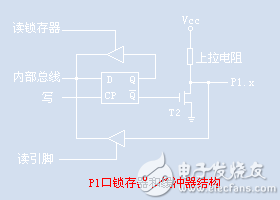
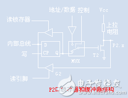
Let's briefly review the quasi-bidirectional IO structure of standard 51.


This quasi-bidirectional IO structure is characterized by
1 The output structure is similar to the OC gate. When the output is low, the internal NMOS is turned on, and the driving capability is strong (800uA); the output high level is supported by the internal pull-up resistor, and the driving capability is weak (60uA).
2 There is always an internal resistor pull-up (except P0 port), the high-level output current capability is very weak, so even if the IO port is short-circuited to ground for a long time, it will not damage the IO port. (Similarly, the IO port has low output capability. , can not be short-circuited to VCC for a long time when outputting low level)
3 When output is output, the output low level can push the LED (also very weak), and the output high level usually requires an external buffer circuit (so the LED is mostly common).
Five, AVR microcontroller IO port (starting from a thousand calls)
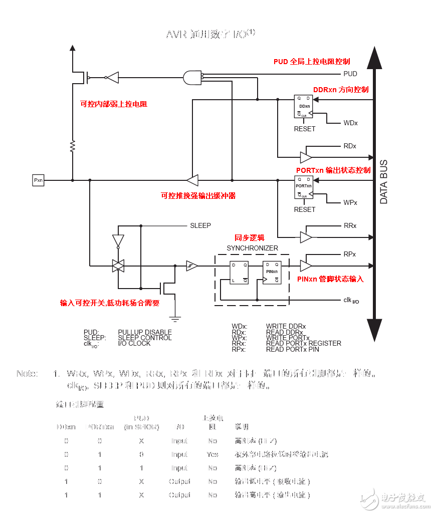
Port pin configuration
DDxn PORTxn PUD (in SFIOR) I/O Pull-up Resistor Description
0 0 X Input No High impedance state (Hi-Z)
0 1 0 Input Yes Output current when pulled low by external circuit
0 1 1 Input No High impedance state (Hi-Z)
1 0 X Output No Output low level (leakage current)
1 1 X output No output high level (source current)
///////////////////////////////////////////////////

Input status:
First, pull-up input status:
1. When the IO port line is left floating, the value of PINxn is 1 and the state is stable.
2. When the input signal is externally connected to the IO port line, the value of PINxn read varies with the high and low level of the external signal. 2. High-impedance input state:
1. When the IO port line is left floating, the value of PINxn is 0, and it is very easy to be scratched. The state is very unstable.
2. External pull-up resistor, the value of PINxn read when the input signal is externally connected to the IO port line changes with the high and low level of the external signal (equivalent to the internal pull-up resistor)
Output status:
In the output state, PORTxn=0, the output is low, and PORTxn=1, the output is high.
1. Output low level, the value of PINxn read when the IO port line is floating is 0.
2, output low level, IO port line connected to VCC or strong pull-up (refers to the pull-up resistance is small, equivalent to direct connection VCC, can provide enough pull-up current) when reading PINxn value is 1
3. Output high level, the value of PINxn read when the IO port line is floating is 1
4, output high level, IO port line connected to GND or strong pull-down (refers to the pull-down resistance is very small, equivalent to directly connected to GND, can absorb enough pull-down current) when reading the value of PINxn 0
Since DDRxn can be configured anyway, we can read the PINxn value. In summary, when we read the value of PINxn, we need to get a correct and stable value.
Should be selected in the internal pull-up input or high-impedance input and external pull-up. Of course, it is also possible to select the internal pull-up input and the external pull-up method, but it is meaningless to add pull (repeated pull-up) both internally and externally.
Another point is that when we read the level given by the software, we need to insert a NOP before reading the PINxn value.
That is to say, a NOP should be inserted in the middle of the value of the output after the IO port outputs the logic level.
///////////////////////////////////////////////////////
The real bidirectional IO structure of AVR is much more complicated. The registers of the control port alone also have 4 PORTx.DDRx, PINx, SFIOR (PUD bit), but the function is also much stronger.
When used as a general purpose digital I/O, all AVR I/O ports have true read-modify-write capabilities.
This means that changing the direction of certain pins (or port level, disable/enable pull-up resistor) with SBI or CBI instructions does not inadvertently change the direction of other pins (or port level, disable/make Can pull up the resistor).
The output buffer has a symmetrical drive capability that can output or sink large currents and directly drive the LEDs.
All port pins have voltage-independent pull-up resistors.
There is a protection diode connected to VCC and ground.
* (Many digital devices have protection diodes, which should be considered in the case of low power applications.)
Each port has three I/O memory addresses:
Data Register – PORTx
Data Direction Register – DDRx
Port input pin – PINx.
The data register PORTx and the data direction register DDRx are read/write registers, and the port input pin PINx is a read-only register.
However, it is important to note that writing a logic "1" to a bit in the PINx register will cause the data in the corresponding bit of the data register to alternate between "0" and "1".
The pull-up resistors for all port pins are disabled when the pull-up disable bit, PUD, of the MCUCR register is set.
When switching between the high state ({DDxn, PORTxn} = 0b00) output state ({DDxn, PORTxn} = 0b11), the (high-impedance) tristate ({DDxn, PORTxn} = 0b11)
Pull-up resistor enable ({DDxn, PORTxn} = 0b01) or output low ({DDxn, PORTxn} = 0b10) There must be one of these two modes.
In general, pull-up resistor enable is fully acceptable because the high-impedance environment does not care whether it is a strong high output or a pull-up output.
If this is not the case, the pull-up resistors of all ports can be disabled by setting the PUD of the SFIOR register.
Switching between pull-up input and output low also has the same problem.
The user must select the high-impedance state ({DDxn, PORTxn} = 0b00) or the output high level ({DDxn, PORTxn} = 0b10) as an intermediate step.
When switching from high-impedance state to output high-level conversion, PUD should be set first, then PORTxn is set to 1, and then DDRxn is set to 1, which means that the high-impedance state is entered first during the conversion process. It can avoid the occurrence of two modes of pull-up resistor enable and output low level)
When switching from output high level to high impedance state, PUD should be set first, then DDRxn should be set to 0, and then PORTxn should be set to 0, that is, the high impedance state will be entered first during the conversion process. It can avoid the occurrence of two modes of pull-up resistor enable and output low level)
When the pull-up input is switched to the output low-level conversion, PORTxn should be set to 0 first, then DDRxn should be set to 1, that is, the high-impedance state is first entered during the conversion process (so that the output high-level mode can be avoided. )
When the output low level is switched to the pull-up input conversion, DDRxn should be set to 0 first, then PORTxn should be set to 1, that is, the high-impedance state is first entered during the conversion process (so that the output high-level mode can be avoided. )
In summary, if we have strict level status requirements during the conversion process, in order to avoid other short-lived states, we must first enter the high-impedance state during the conversion process.
///////////////////////////////////
Regardless of how DDxn is configured, the pin level can be obtained by reading the PINxn register.
Each bit of the PINxn register forms a synchronizer with the latch in front of it.
This avoids signal instability due to pin level changes in a short time range in which the internal clock state changes.
The disadvantage is the introduction of delays.
AVR IO has multiple IO modes:
1 High-impedance state, mostly used for high-impedance analog signal input, such as ADC digital-to-analog converter input, analog comparator input
2 weak pull-up state (Rup=20K~50K), input. Optimized for low level signal input, eliminating external pull-up resistors, such as key input, low level interrupt trigger signal input
3 Push-pull strong output state, strong driving ability (>20mA), can directly push LED, and high and low driving ability is symmetrical. The maximum sinking current can reach 40mA. But it is better to select 20mA when selecting the resistance value.
Precautions for use:
Write with PORTx, read with PINx
During the experiment, try not to connect the pin directly to GND/VCC. When the setting is improper, the IO port will output/fill a large current of 80mA (Vcc=5V), resulting in device damage.
When making input:
1 The internal pull-up resistor is usually enabled, and the floating (high-impedance state) will be easily disturbed. (The surface seems to be 51's strong anti-interference ability, because 51 always has internal resistance pull-up,)
2 Try not to let the input float or the analog input level is close to VCC/2, which will consume too much current, especially for low-power applications. CMOS circuit features
3 When reading the pin level given by the software, there is a clock cycle interval between the assignment instruction out and the read instruction in, such as the nop instruction. (This should be remembered otherwise the program will go wrong)
The input of the 4 function module (interrupt, timer) can be a low level trigger or a rising edge trigger or a falling edge trigger.
5 For high-impedance analog signal input, remember not to enable internal pull-up resistors, affecting accuracy. Such as ADC digital-to-analog converter input, analog comparator input,
At reset:
The internal pull-up resistor will be disabled on reset. If the application (such as motor control) requires strict level control, use an external resistor to fix the level
When sleeping:
For output, it remains unchanged
Input is generally invalid, but if the second function is enabled (interrupt enable), its input function is valid. For example, the wake-up function of an external interrupt.
AVR C language IO operation:
AVR's C language is based on ANSI C. It does not extend bit operations (Boolean operations) like 51. Although there are SBI/CBI/SBIC/SBIS instructions in the assembly instructions, it is necessary to implement bit logic operations. This is a must.
The IO port operates in the same way as the function register, but has special requirements for reading and writing some function registers. Please refer to the manual.
It is not necessary to consider the issue of code efficiency. If possible, GCCAVR will automatically optimize to SBI/CBI/SBIC/SBIS instructions, which is the same as assembly efficiency.
For example, iom16.h defines #define PA7 7
(This standard header defines all official definitions of the MCU (including registers, bits, interrupt entries, etc.), but the second function of the pin is not defined)
I want PA7 to be 1 PORTA"=(1<I think PA7 is 0 PORTA&=~(1<I want PA7 to be inverted PORTA^=(1< want to check if PA7 is 1 if (PINA&(1< want to check if PA7 is 0 if! (PINA&(1<* << is the left shift operator. If you don't understand, you should review the C language foundation.
Note the order of IO operations:
//Power-on default DDRx=0x00, PORTx=0x00 input, no pull-up resistor. Suppose the PA port drives the LED's negative pole and the low level light is on. Initialization method 1:
PORTA=0xFF; //Internal pull-up, high level
DDRA=0xFF; //Output high---------The light is always off Initialization method 2:
DDRA=0xFF; //output low--------the light is lit incorrectly
PORTA=0xFF; //Output high-------- is immediately extinguished, the time is very short (1 command less than uS time), the light flashes, the eyes can not detect
But what if this IO port is to control the ignition signal of the explosive pack? Industrial control should consider the issue of reliability
Tips for simulating the IIC bus of the OC structure:
Although most of the AVRs have a hardware IIC interface, there are cases where it is necessary to use software to simulate IIC. The IIC bus of the OC structure can be realized by using an external pull-up resistor + control DDRx.
The speed of IIC is related to the pull-up resistor. The internal pull-up resistor has a large resistance (Rup=20K~50K), which can only be used in low speed applications.
#define SDA 0 //PC0
#define SCL 1 //PC1
(Program initialization settings SDA and SCL are both PORT=0, DDR=0)
#define SDA_0() DDRA|=(1<#define SDA_1() DDRA&=~(1<#define SCL_0() DDRA|=(1<#define SCL_1() DDRA&=~(1<
Use the SDA_0()/SDA_1()/SCL_0()/SCL_1() macro above to be intuitive, and the efficiency is the same as assembly.
Twinkle System Technology Co Ltd , https://www.pickingbylight.com