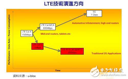
The long-term evolution plan (LTE) high-speed and low data rate double-track development is increasingly clear. In order to promote LTE synchronization to meet high-bandwidth mobile devices and low-rate, low-cost IoT applications, the 3rd Generation Partnership Project (3GPP) has been actively launched in addition to continuing to promote high-speed standards such as Cat. 9/10/11. The development of the LTE Machine Type Communication (MTC) standard will extend the LTE power map to various application areas of the Internet of Things.
At present, all advanced countries are competing to develop B4G (Beyond 4G) and 5G technologies with the requirements of “large capacity, large bandwidth, large link, low latency, low power consumptionâ€. It is estimated that 3GPP will establish 5G Study Item in advance in 2016. Expand the 5G standard development. Since network gateways, mobile devices and in-vehicle infotainment (IVI) systems require high network bandwidth and transmission speed to support video streaming applications, 3GPP is continually renovating LTE-A carrier aggregation (CA). ), MIMO and other technical specifications, the phase gradually achieves a rate of 600 Mbit / s, 1 Gbit / s or more.

Compared with the LTE and LTE-A high-speed mobile networks, the LTE R12 version of the MTC protocol architecture is quite streamlined and can be described as tailored for IoT M2M applications. It is mainly divided into the sensing layer, the network layer and the application layer. The operation process is based on the sensor to extract environmental information, and then transmitted by using LTE Cat. 1/0 technology or bridging to various wireless local area network (WLAN) technologies. Finally, through the application layer in series with various cloud application services, device-to-device communication can be realized at a lower cost, and the data burden of the telecom core network can be alleviated.
Following Cat. 1/0, 3GPP is scheduled to release the Release 13 standard from 2015 to 2016, further importing the Cat.00 (200kbit/s) MTC solution with lower transmission rate, which will reverse the stereotype of LTE biased high-speed network. Impressions, machine-to-machine (M2M) sensing, communication, computing and instant control applications at lower design costs.
LTE MTC not only helps reduce M2M development costs, but also further implements D2D applications such as shop floor communication (V2V), making the Internet of Things more intelligent and continuous. At present, the technology is still in the early stage of discussion, including standards and test specifications have not been adjusted, coupled with the wafer supply chain has not yet been strong, the fastest must also take 1-2 years of design, filming, production and testing processes, pre- It is estimated that relevant solutions will be available from 2016 to 2017.
Usually,10 & 20 layers PCB are HDI board,but some are not .Some with big trace width and space,holes are over 0.3mm too. We have much experience in doing 10 Layer PCB & 20 layer PCB.
A ten-layer board should be used when six routing layers are required. Ten-layer boards, therefore, usually have six signal layers and four planes. Having more than six signal layers on a ten-layer board is not recommended. Ten-layers is also the largest number of layers that can usually be conveniently fabricated in a 0.062" thick board. Occasionally you will see a twelve-layer board fabricated as a 0.062" thick board, but the number of fabricators capable of producing it are limited..
High layer count boards (ten +) require thin dielectrics (typically 0.006" or less on a 0.062" thick board) and therefore they automatically have tight coupling between layers. When properly stacked and routed they can meet all of our objectives and will have excellent EMC performance and signal integrity.
A very common and nearly ideal stack-up for a ten-layer board is shown in Figure 12. The reason that this stack-up has such good performance is the tight coupling of the signal and return planes, the shielding of the high-speed signal layers, the existence of multiple ground planes, as well as a tightly coupled power/ground plane pair in the center of the board. High-speed signals normally would be routed on the signal layers buried between planes (layers 3-4 and 7-8 in this case).
10 Layer PCB
10 layer PCB 10 layer TG170 PCB 10 layer design
Storm Circuit Technology Ltd , https://www.stormpcb.com