In many industrial applications, small differential voltages are required to detect high currents to achieve current monitoring. However, in the case of high common mode voltage, the detection circuit of the output current is complicated, and the accuracy is difficult to ensure. The new high-side current sensor AD8205 simplifies its detection circuitry and greatly improves the accuracy of its detection and control.
The AD8205 is a single-supply, high-performance differential amplifier from Analog Devices, Inc., with a typical single-supply voltage of 5V and a common-mode voltage input range of -2 to 65V, which can withstand an input common-mode voltage of -5 to +70V. It is suitable for industrial equipment that detects small differential voltages with high common mode voltage. It has a fixed gain of 50V/V, an operating temperature range of -40 to +125°C, an offset voltage drift of less than 15V/°C, and a gain drift of less than 30ppm/°C (ambient temperature up to 125°C) over the entire specified temperature range. It has excellent DC performance and has a common mode rejection ratio of up to 80dB from DC to 100kHz. Therefore, its measurement loop error is small and its precision is very suitable for control systems such as motor control, transmission control, magnetic levitation control, vehicle power control, fuel injection control, engine management and DC-DC conversion.
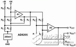
Internal circuit structure and its working principleThe internal circuit of the AD8205 consists of two integrated op amps A1 and A2 and a resistor network, as well as a small reference voltage source and bias circuit. The circuit structure is shown in Figure 1.

Figure 1 Schematic diagram of the internal circuit of the high-side current sensor AD8205
The preamplifier of A1 consists of resistors RA, RB, and RC that attenuate the common-mode voltage to the appropriate input voltage range. The two sets of attenuators form a bridge network with a decay rate of 1/16.7. After the input signal is attenuated, the amplitude of the input signal is kept within the power supply voltage range. When the input voltage exceeds the power supply voltage or is lower than the common ground voltage, the internal reference voltage acts, so that the amplifier inputs a negative common-mode voltage. The signal still works normally. When the bridge is balanced, the differential input signal generated by the common mode voltage signal is 0V. Of course, the input network also attenuates the input differential voltage signal. Amplifier A1 amplifies the attenuated signal by a factor of 26. The input and output are differentially used to obtain the maximum AC common-mode rejection ratio. In addition, the resistance matching ratio of the resistors RA, RB, RC, RD and RF after laser calibration is better than 0.01%. This high-precision calibration enables the device to achieve a common mode rejection ratio of over 80dB.
Amplifier A2 converts the differential signal output from A1 into a single-ended signal and amplifies it by 32.15 times. The reference inputs VREF1 and VREF2 are connected to the non-inverting input of A2 via resistor RREF so that the output can be arbitrarily adjusted to the desired output voltage range. When the two reference inputs are used in parallel, the reference voltage has a gain of 1V/V from input to output; when any of the reference inputs is used alone, the gain is 0.5V/V. The total gain of the AD8205 consists of the attenuation rate of the attenuation circuit of 1/16.7, the amplification factor of A1 of 26, and the amplification factor of 32.15 of A2. The AD8205 has a 300μA pull-down current capability and is connected to a pull-up resistor using a Class A PNP.
Output mode sets unipolar outputThis method is generally used to measure the unidirectionally varying current flowing through the sampling resistor. There are two basic modes: ground reference and V+ reference output mode. In unipolar mode of operation, when the differential input is zero, the output can be biased to a negative (near ground) or positive peak (V+). When a differential voltage is applied to the input, the output will move in the opposite direction to the peak. At this time, the amplitude of the input differential voltage corresponding to the full-scale output is close to 100mV, and its polarity is determined by the static setting of the output voltage. When biased to the positive peak, the input differential voltage should be negative and the output falling from the positive peak; conversely, if statically biased to ground, the input differential voltage should be positive and the output rising from zero.

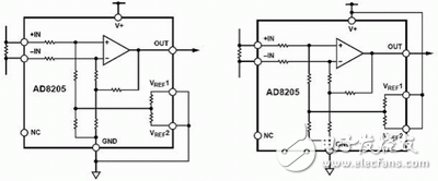
(a) reference to ground (b) reference to V+ Figure 2 unipolar output connection
The ground connection reference connection is shown in Figure 2(a). Its two reference inputs are connected to ground. When the input differential voltage is zero, its output is biased to the inverted peak (about 0.05V).
The output connection method based on V+ is shown in Figure 2(b). Its two reference inputs are connected to the positive supply. When the input differential voltage is zero, its output is biased to the positive phase peak (approximately 4.8V).
Solar water heating (SWH) is heating water by sunlight, using a solar thermal collector. A variety of configurations is available at varying cost to provide solutions in different climates and latitudes. SWHs are widely used for residential and some industrial applications.
Solar Water Heater includes:
- Pressurized Flat Solar Water Heater
- Pressurized Tube Solar Water heater
- Unpressurized Flat Solar Water Heater
- Unpressurized Flat Solar Water Heater
Solar Hot Water Heater,Sun Heater,Solar Powered Water Heater,Solar Water Heater For Home
NANTONG RONGCHANG IMPORT&EXPORT CO.,LTD , https://www.ergsolarcn.com